
Sample-And-Hold Circuit I Circuit

The sample-and-hold circuit is an essential component in various analog-to-digital conversion applications. Its primary function is to capture and hold a specific voltage level from an input signal for a predetermined period, allowing for accurate sampling of rapidly changing signals.
In a typical sample-and-hold circuit, the input signal is fed into a switch, which can be implemented using electronic devices such as Field Effect Transistors (FETs) or other suitable switching elements. When the switch is closed, the circuit samples the input voltage, and upon opening the switch, the sampled voltage is held constant at the output. This output can then be processed by an analog-to-digital converter (ADC) or any other subsequent circuitry.
The hold capacitor is a crucial component in this configuration, as it stores the sampled voltage. The choice of capacitance value is critical; it must be sufficiently large to maintain the voltage level without significant droop during the hold time. The circuit may also incorporate buffer amplifiers to prevent loading effects and ensure that the output impedance remains low, facilitating better interfacing with subsequent stages.
In practical applications, the switching mechanism can be designed to minimize charge injection and leakage currents, which are vital for maintaining the integrity of the sampled signal. The use of FETs as switches is advantageous due to their high input impedance and low power consumption, making them suitable for high-speed and low-noise applications.
Overall, the sample-and-hold circuit is a fundamental building block in modern electronic systems, enabling accurate signal processing in various fields, including telecommunications, instrumentation, and data acquisition systems. This circuit demonstrates the principle of the sample-and-hold circuit. SI can be replaced by electronic switches (FET, etc.) in an actual application.
Related Circuits
The development of the entire system necessitated a thorough identification of all processes related to the laser controller. The initial diagram outlines the primary physical components utilized in the CNC laser system. The setup includes a power supply, a...
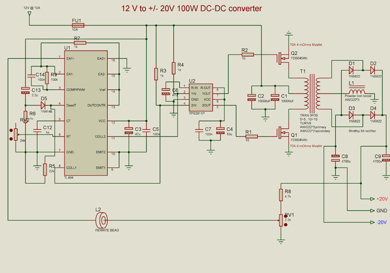
A DC to DC converter circuit is designed to convert a DC voltage to another DC voltage with different levels. This specific converter transforms a +12 V DC input into a symmetrical output of +/-20 V DC. Such circuits...
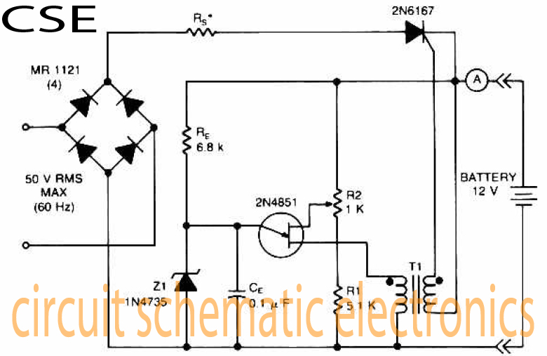
The accumulator charger circuit must provide a voltage that matches the specifications of the batteries being charged. For a 12-volt accumulator, the output voltage should not exceed 12 volts, nor should it fall significantly below this threshold. Failure to...
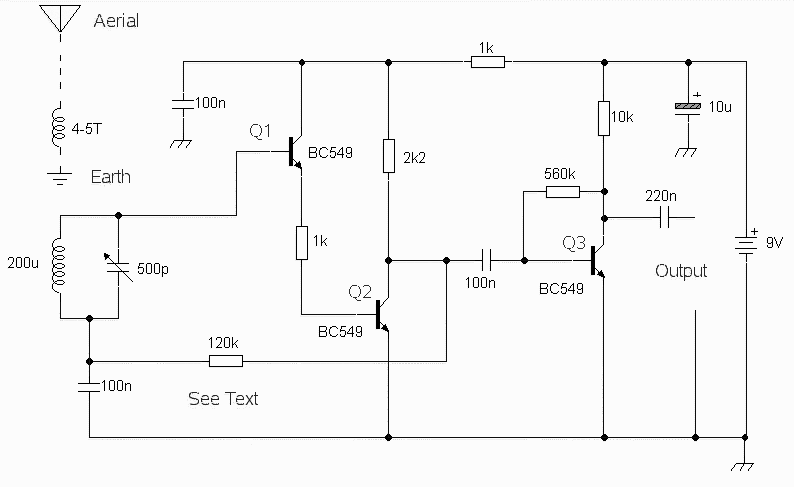
The circuit was designed to obtain signals through amplitude modulation, exhibiting good sensitivity and selectivity. Amplitude modulation. The amplitude modulation (AM) circuit is engineered to effectively capture and process radio frequency signals. The design focuses on achieving high sensitivity, allowing...

This circuit is a touch switch circuit, similar to a touch door alarm. It utilizes a 555 timer as the core component of the touch switch circuit. The operation begins when the plate is touched, triggering the 555 timer....
Figure 1.88 illustrates the loudness control circuit utilizing multiple taps on a potentiometer. In Figure (A), the connection is made between the tap and the potentiometer's input, along with the ground. An RC compensation network is employed, where the...