
12V Solar Charge Controller Circuit

The Low Dropout Voltage (LDO) solar charge controller is designed to optimize the charging of batteries from solar panels while maintaining a low voltage drop across the regulator. The core of the circuit includes a differential amplifier that monitors the output voltage and compares it to a reference voltage. This comparison allows the amplifier to adjust the gate voltage of the P-channel MOSFET, which acts as a linear regulator.
In this configuration, the P-channel MOSFET is placed in series with the load, allowing it to effectively regulate the output voltage to the battery. The LDO design is particularly advantageous in scenarios where the input voltage from the solar panel is only slightly higher than the battery voltage, as it minimizes power loss and heat generation.
The operational principle involves the differential amplifier continuously adjusting the MOSFET gate to maintain a stable output voltage, even as the solar panel output fluctuates due to changing light conditions. This ensures that the battery is charged efficiently without overcharging, which could lead to battery damage.
The circuit may also include additional components such as capacitors for filtering, diodes for reverse polarity protection, and resistors for setting reference voltages. These components enhance the reliability and performance of the charge controller, making it suitable for various solar energy applications, including small solar-powered devices and larger solar energy systems.
Overall, the LDO solar charge controller represents a practical solution for efficient solar energy management, leveraging simple yet effective electronic components to achieve optimal performance.This Low Dropout Voltage (LDO) solar charge controller uses a simple differential amplifier and series P channel MOSFET linear regulator --their compatibil.. 🔗 External reference
Related Circuits
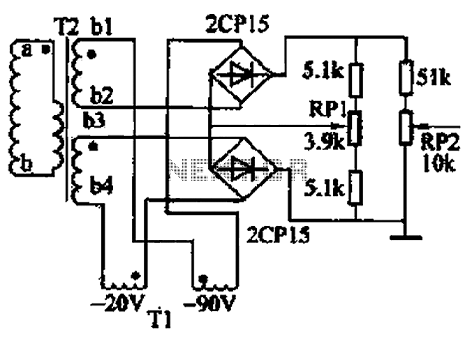
The closed-loop system consists of longitudinal and transverse components. The circuit operates as follows: a control circuit from the stepping motor CNC system issues a command, which the receiver detects. This signal is processed through a phase-sensitive rectifier to...
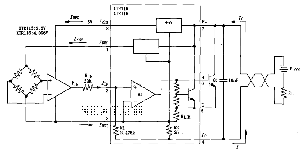
The output reference voltage VREF from the O pin is not utilized within the internal circuit; instead, it is provided to the external circuit. Similarly, the output voltage VREG is also supplied to the external circuit. All current return...
This article presents a high reliability 1200V High Voltage Integrated Circuit (1200V HVIC) for half bridge driver applications, aimed at reducing the IC's supply current by approximately 50%. The 1200V High Voltage Integrated Circuit (HVIC) is designed specifically for half-bridge...

Active speaker with amplifier circuit TDA1521 and NE5532, featuring dual-channel input and dual-channel output. The active speaker circuit utilizes the TDA1521 integrated circuit, which serves as the power amplifier. This IC is designed for high-efficiency amplification, providing a robust output suitable...
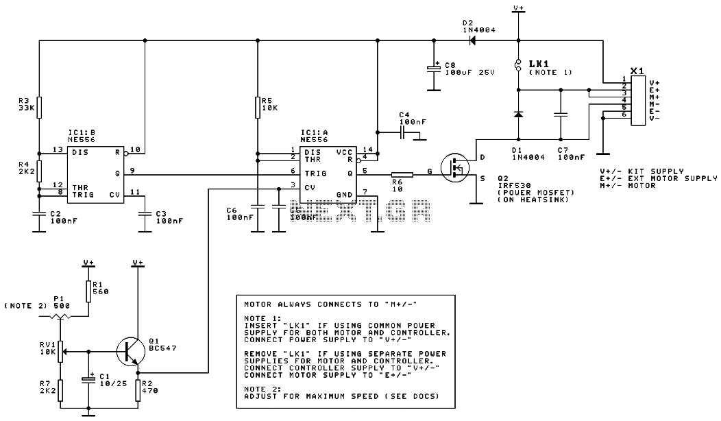
This is the schematic diagram of a DC motor speed controller circuit. The circuit utilizes two oscillators/timers that are configured as a Pulse Width Modulator (PWM). The timer chip used in this circuit is a dual NMOS timer/oscillator. The DC...
This page describes a battery tester designed to characterize batteries and save the results on a microSD card. The battery tester circuit is engineered to evaluate the performance and capacity of various battery types, providing accurate and reliable data storage...