
3V to 40 Volt DC Converter Circuit

The MC34063 series switching regulator is a highly versatile and efficient solution for converting DC voltage levels. This device operates within a wide input voltage range, making it suitable for various applications, from battery-powered devices to industrial equipment. Its ability to provide outputs that can exceed, match, or invert the input voltage is particularly beneficial in systems where different voltage levels are required.
The internal architecture of the MC34063 includes a temperature-compensated reference voltage, which ensures stable operation across varying temperature conditions. The comparator monitors the output voltage and adjusts the duty cycle of the oscillator accordingly, maintaining the desired output level. The controlled duty cycle oscillator is a critical component that manages the switching frequency of the regulator, optimizing efficiency while minimizing heat generation.
The active peak current limit circuit is an important safety feature that protects the device from overcurrent conditions, enhancing the reliability of the circuit. The high current output switch allows for efficient power delivery to the load, enabling the regulator to support higher current applications without significant losses.
This device is housed in an 8-pin dual in-line package (DIP), facilitating easy integration into various circuit designs. The pin configuration allows for straightforward connections to input voltage, output voltage, ground, and feedback paths, simplifying the design process for engineers. Overall, the MC34063 series switching regulator is an excellent choice for applications requiring efficient DC to DC conversion with flexible output options.Switching regulator subsystems intended for use asdc to dc converters. 3V to 40 Volt DC Converter circuit | The use of switching regulators is becoming more pronouncedover that of linear regulators because the size reductions innew equipment designs require greater conversion efficiency. Another major advantage of the switching regulator is that it has increasednapplication flexibility of output voltage. The output can be less than, greater than, or of opposite polarityto that of the input voltage. The MC34063 series is a monolithic control circuitcontaining all the active functions required for dc to dcconverters. This device contains an internal temperaturecompensated reference, comparator, controlled duty cycleoscillator with an active peak current limit circuit, driver, and a high current output switch.
This series was specificallydesigned to be incorporated in step up, step down andvoltage inverting converter applications. These functionsare contained in an 8 pin dual in line package. 🔗 External reference
Related Circuits
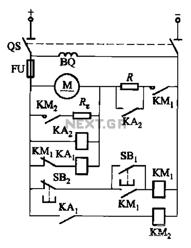
The circuit illustrated in Figure 3-196 features a starting resistance level and an undervoltage relay (KAz) that is controlled by the removal of the startup resistor. It also includes dynamic braking for shutdown purposes. The undervoltage relay (KAL) operates...
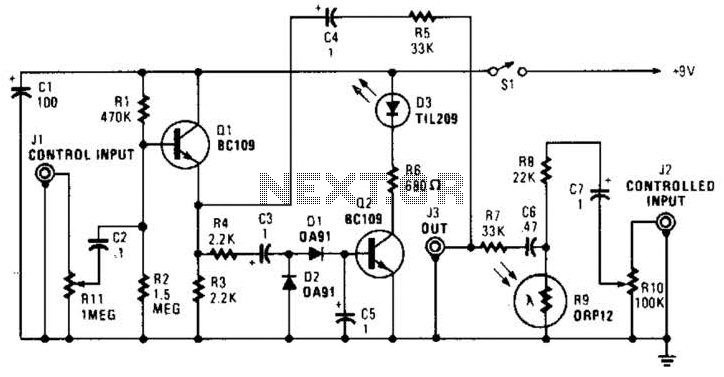
In this circuit, audio input to the control channel is amplified and rectified by diodes D1 and D2. This direct current level activates LED D3 through transistor Q2. The illumination from LED D3 causes R9, a light-dependent resistor, to...
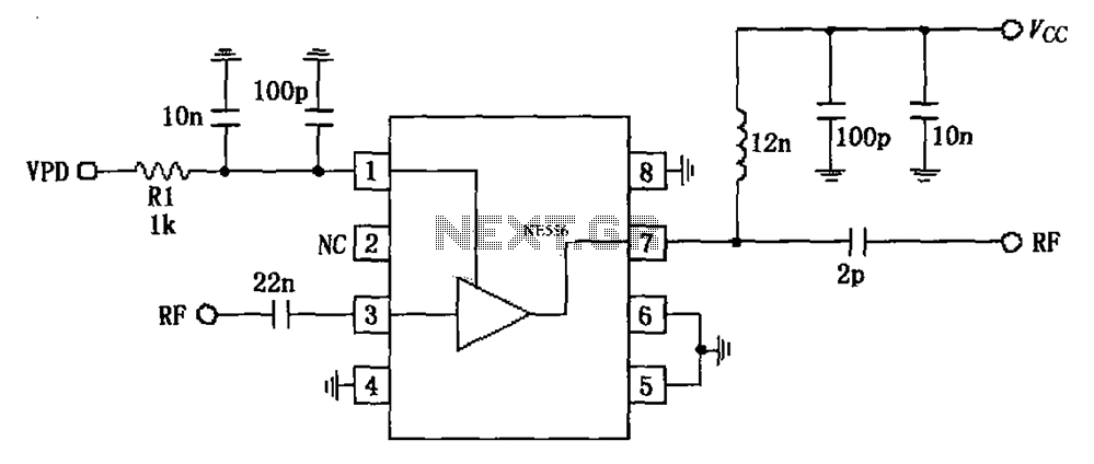
The circuit is based on an 880 MHz RF2347 low noise amplifier application. The radio frequency (RF) signal enters through input pin 3, and after amplification, the output is available at pin 7. The amplifier is directly coupled to...
Many households are still equipped with tube-type television sets. If there is a desire to connect one of these large televisions to a stereo system to enhance the sound quality... To connect a tube-type television to a stereo system, it...
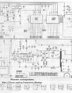
Circuit for Grundig 5441 TV. If there are any issues related to this circuit, please provide additional information about the problem for further assistance. By accessing the Fixya site, users acknowledge that they have read and agreed to its...
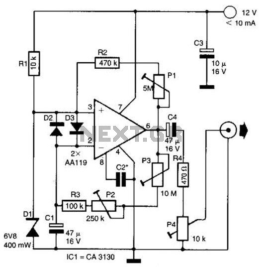
This circuit generates noise pulses suitable for test purposes. A Zener diode serves as the noise source. IC1 functions as a relaxation oscillator. P1 determines the noise bandwidth, while P2 and P3 control the noise amplification. The current consumption...