
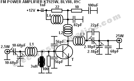
3W FM Transmitter Circuit

The FM transmitter circuit is designed to operate efficiently within the specified frequency range, utilizing components that facilitate optimal signal transmission and reception. The core of the circuit typically includes an oscillator stage, which generates the carrier frequency, and a modulator stage that imposes the audio signal onto the carrier wave. The output stage is responsible for amplifying the modulated signal to the desired power level.
In the context of enhancing stability, the addition of a PLL can significantly improve frequency accuracy and reduce drift, which is particularly beneficial for applications requiring precise frequency control. The PLL works by continuously comparing the output frequency with a reference frequency and adjusting the oscillator accordingly to maintain a locked condition.
The BLY88 amplifier, noted for its high power output capabilities, is integrated into the circuit to boost the signal strength further. This combination allows for effective transmission over longer distances, making it suitable for various applications, including community broadcasting or personal use.
The circuit's performance has been validated under practical conditions, with an SWR measurement indicating efficient power transfer from the transmitter to the antenna. An SWR value of 1:1.05 suggests minimal reflected power, which is crucial for maintaining the longevity of the transmitter and ensuring optimal performance.
Constructing the transmitter requires careful attention to detail, particularly in the layout of the circuit board and the selection of components. RF shielding is essential to minimize interference and ensure that the transmitted signal remains clean and undistorted. Proper grounding techniques and the use of high-quality connectors and cables will further enhance the overall performance and reliability of the transmitter system.
In summary, this FM transmitter schematic offers a robust solution for achieving reliable and efficient transmission within the specified frequency range, with considerations for stability and signal integrity through the potential integration of a PLL and careful construction practices.This is the schematic for an FM transmitter with 3 to 3. 5 W output power that can be used between 90 and 110 MHz. Although the stability isn`t so bad, a PLL can be used on this circuit. This is a circuit that I`ve build a few years ago for a friend, who used it in combination with the BLY88 amplifier to obtain 20 W output power. From the notes tha t I made at the original schematic, it worked fine with a SWR of 1 : 1. 05 (quite normal at my place with my antenna). 2. The circuit has been tested on a normal RF-testing breadboard (with one side copper). Make some connections between the two sides. Build the transmitter in a RF-proof casing, use good connectors and cable, make a shielding between the different stages, and be aware of all the other RF rules of building. 🔗 External reference
Related Circuits

The schematic closely resembles the one found in the CPLD Development Board Tutorial, as it is essentially the same board with a minor addition. The new components are located in the lower right corner, including eight DIP switches, a...
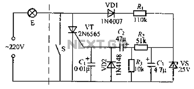
A delay circuit using an improved quenching lamp pull switch is described, focusing on its performance and the delay function in lighting control. The circuit exhibits a high degree of stability and reliability. When switch S is closed, the...
This 300W RF power amplifier for an FM transmitter utilizes 2 x TP9383 transistors. It operates within the 88 - 108 MHz frequency band. The 300W RF power amplifier is designed specifically for FM transmission applications, providing high power output...

Radio-frequency schematics (also see NE602 datasheet and application note). This page contains electronic circuits related to RF receivers. This index features a broad collection of RF receiver circuits. Radio-frequency (RF) schematics are essential for designing and implementing circuits that operate...
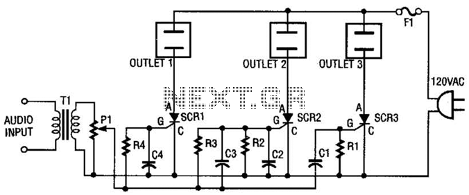
The AC line power is introduced into the circuit through F1, a protective 5-A fuse. One side of the AC line is connected to one side of each AC outlet, while the other side is connected to each silicon-controlled...

Standard LED flashers activate the LED in a rapid on-off sequence, which can become bothersome over time. The circuit presented here offers a more gradual illumination effect. This circuit utilizes a simple design to create a soft flashing LED effect,...