
555 timer bassed Electronic lock circuit with explanation

The circuit design utilizes a 555 timer in monostable mode, allowing for a straightforward yet effective key code lock mechanism. The selection of components such as resistors and capacitors is critical for ensuring the timing requirements are met. The operational sequence begins with the simultaneous pressing of switches SA and SC, which initiates the charge cycle of capacitor C3. The choice of resistor values R3 and R4 is crucial, as they form a voltage divider that dictates the charging time of C3, allowing for a predetermined delay before the next step in the unlocking sequence can be executed.
Once the initial switches are released, the discharge of C3 through R4 is monitored, and the timing is set to ensure that the subsequent switch presses (S1 and S8) occur within the five-second window. This aspect of the design adds a layer of security, as it requires precise timing and coordination from the user. The triggering of the 555 timer at pin 2 leads to a high output at pin 3, which is responsible for activating the relay that controls the locking mechanism.
The relay's integration into the circuit allows for the physical actuation of the lock, making this design suitable for various applications where electronic access control is required. The reset functionality provided by the additional switches ensures that any incorrect attempts to enter the code will revert the circuit to its initial state, maintaining the integrity of the locking mechanism. This combination of simplicity, cost-effectiveness, and functionality makes this electronic key code lock circuit a viable solution for basic security applications.A very simple electronic key code lock circuit that require few external components can be constructed using this schematic diagram. This electronic key code lock circuit is based on a common 555 timer circuit and some other common components.
This low cost key code circuit use six switches that needs to be pressed to open the lock, but only two switches at a time. In many other, more expensive electronic circuits the key code is formed by pressing some switches one by one, not like in this case two switches. If you don`t like to press two switches in the same time you can eliminate one switch, but in that case the code can be more easy to guess by someone ells.
An essential property of this electronic code lock is that it works in monostable mode, i. e. once triggered, the output becomes high and remains so for a period of time, governed by the Pin 2 of 555 timer is the triggering input pin which, when held below 1/3 of the supply voltage, drives the output to high state. The threshold pin 6, when held higher than 2/3 of the supply voltage, drives the output to low state.
By applying a low-going pulse to the reset pin 4, the output at pin 3 can be brought to the quiescent low level. Thus the reset pin 4 should be held high for normal operation of the IC. Three sets of switches SA-SC, S1- S8 and S3-S4 are pressed, in that order, to open the lock. On pressing the switches SA and SC simultaneously, capacitor C3 charges through the potential divider comprising resistors R3 and R4, and on releasing these two switches, capacitor C3 starts discharging through resistor R4.
Capacitor C3 and resistor R4 are so selected that it takes about five seconds to fully discharge C3. Depressing switches S1 and S8 in same time, within five seconds of releasing the switches SA and SC, pulls pin 2 to ground and IC 555 is triggered. The capacitor C1 starts charging through resistor R1. As a result, the output (pin 3) goes high for five seconds. The contacts of the relay close and the solenoid pulls in the latch (forming part of a lock) and the lock opens.
The remaining switches are connected between reset pin 4 and ground. If any one of these switches is pressed, the IC is reset and the output goes to its quiescent low state. 🔗 External reference
Related Circuits

This circuit is designed for a project utilizing a 6V, 400 mA DC power supply. The open-circuit voltage is specified, indicating the voltage measured when no load is connected. The circuit employs a regulated 6V power supply, which is essential...
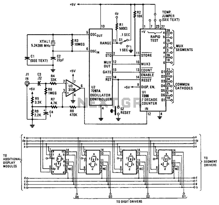
The circuit comprises an ICM7208 seven-decade counter (U1), an ICM7207A oscillator controller (U2), and a CA3130 biFET operational amplifier (U3). Integrated circuit U1 counts input signals, decodes them into a 7-segment format, and outputs signals to drive a 7-digit...

The interface circuit is placed between the computer's standard video signal output terminal and the television. It amplifies the standard 1V (Peak-to-Peak) video signal to 3V (Peak-to-Peak). The negative feedback circuit consists of transistors T1 and T2, providing a...
This circuit design for a low current relay is intended for use in battery-operated electronic devices, with an operating current in microamperes (µA). It utilizes a bistable relay and additional components to enable the relay to function similarly to...
The electronic locust killer device consists of a square wave oscillator circuit and a high-voltage generator circuit, as illustrated in Figure 3-192. The square wave oscillator comprises a counting divider IC, resistors R5 and R6, capacitor C1, and potentiometer...
The VE1 preamplifier utilizes a low muscle, low resistance double triode 6N6 configuration, with separate halves for the left and right audio channels. The design operates within the CPI framework. It promotes the use of high-level VE2 household low...