
555 transistor characteristic curve tracer circuit diagram

The transistor characteristic curve tracer circuit is designed to provide a visual representation of a transistor's performance across various operating conditions. The astable multivibrator configuration formed by the 555 timer and passive components (R1, R2, and C1) generates a continuous square wave signal. This square wave signal modulates the base current (Ib) of the transistor under test, allowing for the examination of its response characteristics.
The sawtooth waveform produced by the integrating circuit (C2 and R3) is crucial in generating a linear ramp voltage that varies over time, which is then used to modulate the collector current (Ic) of the transistor. By connecting the output of the emitter follower (VT4) to an oscilloscope, the user can observe the changes in Ic as the base current is varied, effectively plotting the Ic-Vcc characteristic curve of the transistor.
The ladder wave generator, composed of capacitors (C3, C4) and transistors (VT1 to VT3), facilitates the creation of discrete voltage steps. These steps correspond to different operational states of the transistor, allowing for a detailed analysis of its switching behavior. The controlled charging and discharging of C4 ensure that the circuit can produce a series of well-defined steps, which are essential for accurately mapping the transistor's characteristics.
Finally, the circuit's output is designed to be connected to an oscilloscope, providing a clear visual representation of the IV characteristic curve. This setup allows engineers and technicians to evaluate the performance parameters of transistors, such as current gain, saturation voltages, and cutoff regions, aiding in the selection and application of transistors in various electronic designs. As shown in Figure 555 is the transistor characteristic curve tracer circuit depict transistor characteristics, to have two voltages, one step wave is applied b pole for genera ting different Ib, the second is on the sawtooth c pole, its period staircase corresponds to depict Ic-Vcc characteristic curve. As illustrated, 555 and R1, R2, C1 composition astable multivibrator, the oscillation frequency f 1.44 (R1 + 2R2) C1.
Illustration parameter f 1100Hz. C2, R3 composed of the integrating circuit for generating a ramp, through VT4 emitter follower output, added to the oscilloscope vertical Y and enter the test tube c pole. C3, D1, VT1 ~ VT3, C4 and other components ladder wave generator, every five oscillation cycles, charging voltage on C4 to make VT3 conduction, C4 discharge, formed five steps.
C4 on a single charge, VT2 emitter voltage drops that form a step. Step wave through R4 is added to the test tube b pole. The test tube is figure VTx. After the oscilloscope connected to an IV characteristic curve shown in Figure b.
Related Circuits

This is a simple electronic circuit for a clap switch project. It is suitable for beginner electronics learners who enjoy experimenting with new projects. The circuit can turn on or off a 220V electronic device, such as a fan...
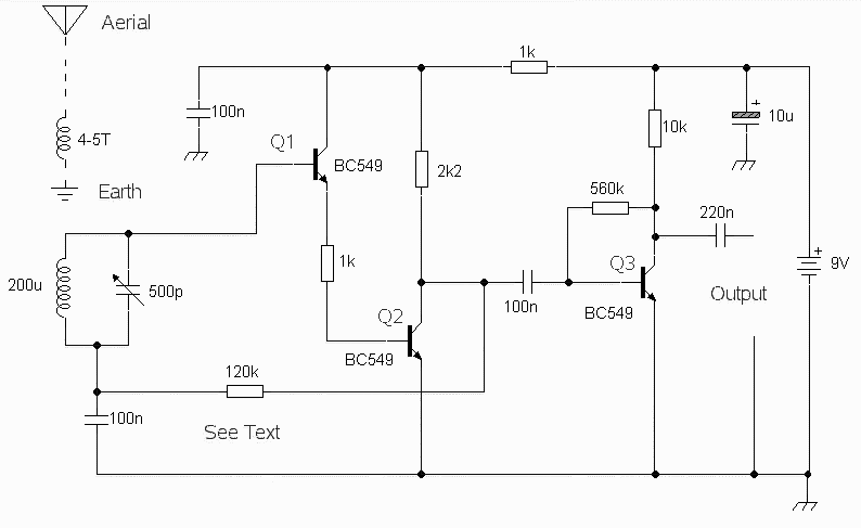
The circuit was designed to obtain signals through amplitude modulation, exhibiting good sensitivity and selectivity. Amplitude modulation. The amplitude modulation (AM) circuit is engineered to effectively capture and process radio frequency signals. The design focuses on achieving high sensitivity, allowing...

The circuit, as illustrated in Figure 3-82, employs a 555 IC to control a motor automatically, managing its start and stop cycles. The running and stopping times of the motor can be adjusted by modifying the values of potentiometers...

This basic PIC-based RS-232 serial interface can control up to 120 digital TTL outputs. The described circuit utilizes a PIC microcontroller to facilitate communication via the RS-232 protocol, which is a standard for serial communication. The interface primarily serves to...
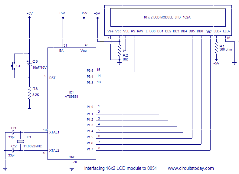
Interfacing a 16x2 alphanumeric LCD module with the AT89S51 microcontroller. The circuit diagram, theory, and program are included. JHD162 LCD module pinout and commands are provided. The integration of a 16x2 alphanumeric LCD module with the AT89S51 microcontroller involves several...

This is a circuit diagram for a solid-state charge detector. It can detect very weak electric fields. The circuit has three components: a 6-volt battery, a light-emitting diode (LED), and a field-effect IC ADM666A. The solid-state charge detector circuit is...