
A watchdog circuit diagram

The described circuit utilizes a CD4060 integrated circuit, which functions as a frequency divider and oscillator. This device is pivotal in generating the timing signals necessary for the operation of the NMOS transistor and the LED. The reset pulse is essential for initializing the CD4060, ensuring that the output states are correctly set before the circuit begins its primary function.
The timing components, including resistors R2 and R3 and capacitor C1, are configured to create a delay that allows sufficient time for the system to stabilize. The choice of these components directly affects the duration of the reset pulse. A longer time constant can be achieved by increasing the values of R2 and C1, thus providing an extended initialization period for the processor circuitry.
The NMOS transistor serves a dual purpose: controlling the LED and acting as a switch that provides power to the processor. When the reset pulse is active, it ensures that the NMOS transistor remains in the conductive state, allowing current to flow through the LED, which indicates that the circuit is powered and operational.
Despite its advantages, the circuit's reliance on a wide pulse width can limit its applications. The design must ensure that the pulse width is adequate to trigger the NMOS transistor consistently; otherwise, the circuit may fail to operate as intended. Therefore, careful consideration must be given to the pulse generation mechanism to ensure reliable performance.
Overall, this circuit design is an effective solution for applications requiring a delayed initialization sequence, provided that the pulse width requirements are met. Its low cost and simplicity make it a suitable choice for various electronic projects.As Figure: when the operation of the circuit as long as the timing of the reset pulse to the CD4060, we can guarantee the state ended in Q1, so that the NMOS transistor control led in the on state power to the processor circuitry. The advantage of this circuit is that the timing of the time can be relatively long, a few minutes no problem, it can take a long time to those who have enough time to initialize the system for initialization. Pulse trigger the dogs, when the power through R2, C1, R3 an automatic reset pulse to the counter to ensure that there is an output Vout.
Circuit costs low.The biggest drawback of this circuit is that the dogs require a relatively wide pulse.
Related Circuits
There have been numerous inquiries regarding this project, primarily due to issues with the source code provided at the end of the author's notes. This problem has been widely reported online, and similar compilation errors have been encountered. It...
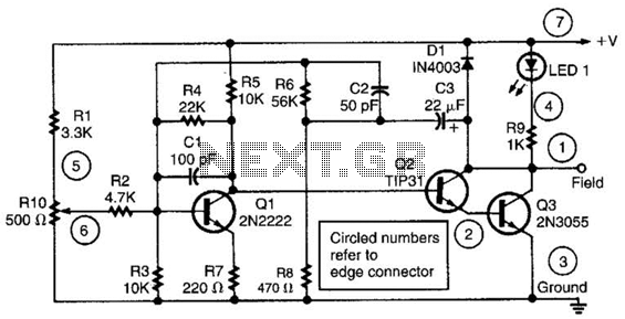
This alternator regulator utilizes a 3-transistor DC amplifier and is designed for a pulled-up field system, where one side of the alternator field returns to the +12V supply, and the other end is pulled toward ground. The circuit monitors...
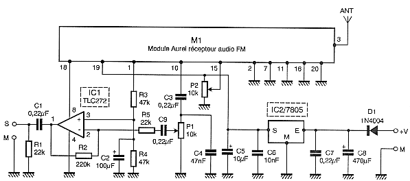
Circuit designed to alleviate concerns related to high frequency utilizes a ready-made module, specifically an Aurel audio FM transmitter. This compact circuit board, measuring 2 cm by 4 cm, supports a modulation frequency track and delivers an RF power...
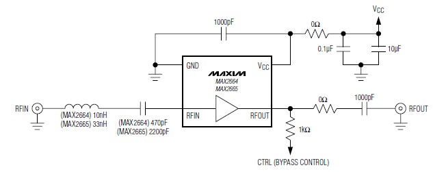
A simple, low-cost, and ultra-compact VHF/UHF low-noise amplifier circuit can be designed using the MAX2664 and MAX2665 ultra-compact LNAs for VHF/UHF applications. These devices incorporate a broadband LNA with an integrated bypass switch. The MAX2664 covers the UHF frequency...
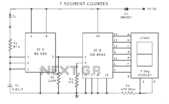
A display counter circuit is illustrated through a diagram featuring a seven-segment display controlled by the counter IC CD4033. This counter circuit is designed to visually represent incremental counts, enhancing its appeal for integration into various applications. An astable...
Figure 1-123 illustrates the internal block diagram of the TDA3810. The circuit is capable of functioning in three operational modes: (1) it can convert a mono channel stereo signal into an analog signal; (2) it can operate in stereo...