
AC/DC 3 digits voltmeter circuit

The voltmeter circuit is designed to accurately measure and convert voltage signals into a digital format. At the core of the input stage is an operational amplifier configured in a peak rectifying mode. The operational amplifier amplifies the input voltage and, through diode feedback, ensures that the output reflects the peak value of the input signal with high linearity. This configuration minimizes distortion and improves the accuracy of the voltage measurement.
Resistors R1 and R2 are employed in a voltage divider configuration, allowing for partial pressure isolation. This arrangement facilitates the scaling of the input voltage before it is fed into the A/D converter. The CA3162E is a dual multi-channel BCD output A/D converter, which digitizes the analog voltage signal and outputs it in a binary-coded decimal format. This is particularly useful for applications requiring precise voltage readings in digital systems.
Furthermore, the circuit allows for the addition of a test voltage ranging from 0 to 1V DC. This feature enables the user to apply a reference voltage to the differential input terminals of the CA3162E, enhancing the versatility of the circuit. The ability to interface with a variety of input signals makes this voltmeter circuit suitable for a wide range of measurement applications in electronics and instrumentation.
Overall, this design effectively combines operational amplification, rectification, and digital conversion to create a reliable and accurate voltmeter circuit.The input stage of this voltmeter circuit uses operational amplifier and diode feedback to form linearity peak value rectifier circuit. Through R2/R2 partial pressure isolation, it is sent to double multi-channel BCD output A/D converter CA3162E, it also can add 0~1V DC tested voltage to CA3162E differential input terminal between ?
and ?, If ? is not used.. 🔗 External reference
Related Circuits
FIG. 284 illustrates a practical emergency power lighting system that activates automatically in the event of a sudden power outage. The fluorescent lights serve as emergency lighting. If the primary illumination lamp is turned off due to a power...
Connect the serial cable to the serial port. If using a USB to TTL, RS232, or serial converter, plug it into the USB port. Next, short the Tx pin to the Rx pin or the TxD pin to the...
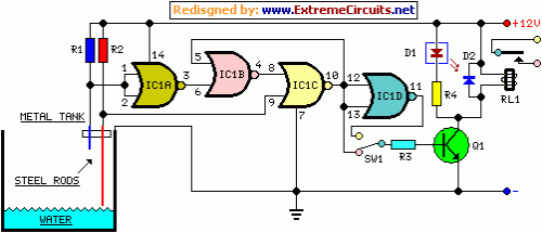
This circuit utilizes a relay to control a water pump, enabling automatic level control for a water reservoir or well. The shorter steel rod acts as the "water high" sensor, while the longer rod serves as the "water low"...
The LM4911 is presented in a configuration that does not utilize an output capacitor (OCL) for its power circuit. This design eliminates the need for squelch control (Mute), as the shutdown control (SD) responds more rapidly than the squelch...

This circuit represents a negative resistance configuration. All previous circuits utilize RC time constants to achieve resonance. LC combinations can also be employed, providing good frequency stability, high Q factor, and rapid startup. In this circuit, a signal input...
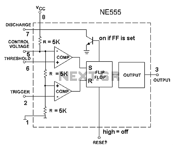
The 555 timer circuit, regardless of the manufacturer, has a consistent internal structure and performance. Various manufacturers produce different models of the 555 timer, including MC555, CA555, XR555, LM555, as well as domestic models like SL555, FX555, and 5G1555....