
Acoustic Field Generator Circuit

The center-channel dialogue filter is constructed by cascading a 3-kHz low-pass filter with a 3-Hz high-pass filter to create a band-pass filter. This filter exhibits a sharp -18 dB/octave cutoff, a flat voltage and power frequency response, and minimal phase change within the passband. In section C, IC3-a and IC3-b form an active crossover network for driving a subwoofer. IC3-a sums signals from the left- and right-channel buffer amplifiers, inverts the summed signal 180 degrees, and provides a low driving impedance for the subsequent filter stage. IC3-b, along with its associated RC network, forms a 75-Hz, 3rd-order low-pass filter. This filter inverts the signal another 180 degrees, ensuring that the signal across resistor R79 (which acts as the output-level control) is back in phase with the original input signal.
The delay section of the AFG, illustrated in D, is based on the MN3008 bucket brigade device (BBD) and the MN3101 two-phase variable-frequency clock generator. The required delay in this system ranges from approximately 5 to 35 milliseconds. The delay time of a BBD is determined by the number of stages divided by twice the clock frequency. Resistors R53, R54, R77, and capacitor C44 are selected to produce a clock frequency, adjustable via R77, which varies from about 30 kHz to 130 kHz. In section A, switch S1 selects the signal to be delayed: either the difference signal (L-R) from IC2-d in matrix mode or the sum signal (L+R) from IC2-c in concert mode. The chosen signal is routed from S1 to the delay section (D), where IC4-d is configured as an inverting amplifier; resistor R75 adjusts the gain between unity and X3. Integrated circuits IC4-a and IC4-b, along with their associated RC networks, are identical 3rd-order 15 kHz low-pass filters. The cascading of these two filters results in a very sharp cutoff (-36 dB per octave). Potentiometer R76 adjusts the bias voltage required by the BBD to precisely one half of the supply voltage, as specified.
The power supply for the AFG, depicted in section G, follows a conventional design. A 25-V center-tapped transformer, along with diodes D1 and D2, provides approximately 18-V unregulated DC. Two 2200 μF filter capacitors ensure sufficient energy storage to meet the high-current demands of the audio output amplifier integrated circuits during high output peaks. Referring to the simplified schematic in A, the AFG is made up of 10 relatively simple circuit elements. ICl-c and ICl-d arc configured as unity-gain noninverting buffer amplifiers. The summing (L+R) amplifier, IC2-c, combines equal amounts of the left and right signals, via R14 and R15, to develop a total composite signal.
Left- and right-channel signals are applied equally through R13 and R12 to IC2-d, the difference (L-R) decoder. Any common to both channels is canceled by IC2-d, which exactly balances the inverting and noninverting gains of the amplifier for a perfect null, The stereo width-enhancement circuit made up from ICl-a and IC`-b works similarly to the (L-R) decoder, except that C25 and C26 have been added in the inverting inputs of each op amp.
ICl-b develops the left wide signal because its inverting and noninverting inputs are connected to the left and right channels opposite that of ICl-a, The output of the width-enhancement circuit is routed to S4, which selects either the wide or the bypass signal for feeding the front-channel amplifier. The center-channel dialogue filter is built by cascading a 3-kHz low-pass filter with a 3-Hz liigh-pass filter to form a band-pass filter. It has a sharp -18 dB/octave cutoff, a flat voltage and power frequency response, and minimum phase change within the passband.
In C, IC3-a and IC3-b form an active crossover network for driving a subwoofer. IC3-a sums signals from the left- and right-channel buffer amps, it inverts the summed signal 180 degrees, and provides a low driving impedance for the following filter stage. IC3-b and its associated RC network form a 75-Hz, 3rd-order low-pass filter. The filter inverts the signal another 180 degrees, so the signal that appears across R79 (which is the output-level control) is back in phase with the original input signal.
The delay section of the AFG, shown in D, is built around the MN3008 bucket brigade device (BBD), arid the MN3101 two- phase variable-frequcncy clock generator. The amount of delay required in this system varies between approximately 5 to 35 milliseconds. The delay time of a BBD is equal to the number of stages divided by twice the clock frequency. Values were chosen for R53, R54, R77, and C44, to produce a clock frequency, adjustable via R77, which varies from about 30 kHz to 130 kHz.
In A, SI selects the signal to be delayed; either the difference signal (L-R) from IC2-d in the matrix mode or the sum signal (L+i) from IC2-c in the concert mode. The selected signal is fed from SI to the delay section (D) where IC4-d is configured as an inverting amplifier; R75 adjusts the gain between unity and X3.
Integrated circuits IC4-a and IC4-b, along with their assoicated RC networks, are identical 3rd-order 15:kHz low-pass filters. Cascading two filters produces a very sharp cut off (-36 dB per octave). Potentiometer R76 adjusts the bias voltage required by the BBD to exactly one half the supply voltage, as required.
The power supply of the AFG, shown in G, is of conventional design. A 25-V center-tapped transformer, along with diodes D1 and D2, produces about 18-V unregulated dc. Two 2200- filter capacitors provide ample energy storage to meet the high-current demands of the audio output amplifier ICs during high output peaks.
Related Circuits
This site addresses a range of subjects pertaining to circuits and electronics. Some of the topics discussed on this site include: * Alternating Relay Switch * Photoswitch Relay. The site serves as a comprehensive resource for understanding various electronic components...
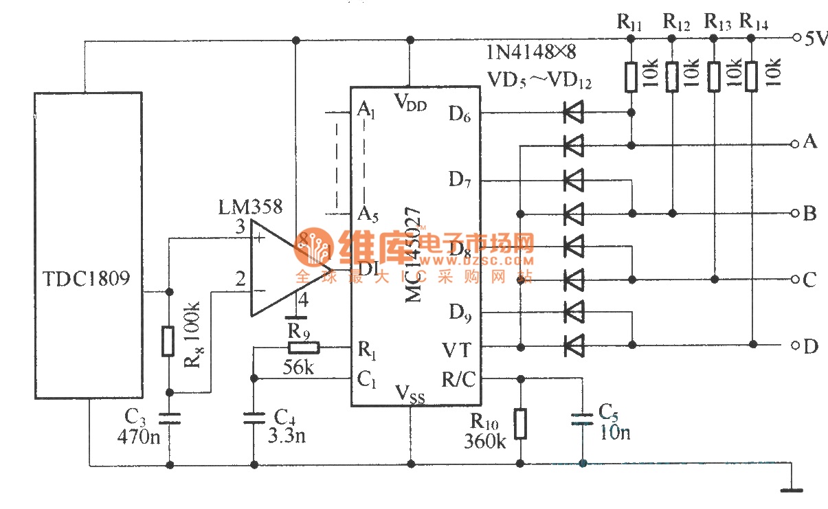
The TDC1808/TDC1809 is a pair of wireless remote control transmitter and receiver components. They utilize an internal antenna to transmit both digital and analog signals. These components are suitable for various wireless remote control devices. Key features include compact...
This circuit is designed to indicate the power output level of any audio amplifier. It is simple, portable, and displays three power levels that can be set to any desired value. The circuit operates by utilizing a combination of resistive...
This circuit is designed to achieve exceptional popularity, as evidenced by its record-breaking views and comments on the referenced website. As of May 3, 2013, it has garnered 760,191 views and 412 comments, with 116 views recorded on that...
Safety polarity connection circuit design using common electronic components The safety polarity connection circuit is designed to ensure that electronic devices are connected with the correct polarity, preventing damage from reversed connections. This circuit typically employs common electronic components such...
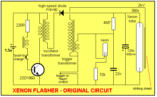
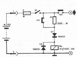
This discussion covers three different Xenon flashing circuits from disposable cameras. From these circuits, unique techniques not found in any theoretical literature will be presented. The first circuit consists of six building blocks. An old disposable flash camera and...