
AD7730 digital pressure measuring circuit

The AD7710, AD7715, and AD7730 are versatile integrated circuits designed for sensor signal conditioning, making them suitable for a variety of applications in data acquisition systems. These ICs feature a digital interface that facilitates communication with microcontrollers or digital signal processors, allowing for seamless integration into complex systems. The control port enables configuration of various parameters, enhancing flexibility in application-specific settings.
The clock generator within these ICs is crucial for synchronizing operations, ensuring accurate data sampling and processing. The digital filter contributes to noise reduction, improving the quality of the signal before it undergoes further processing. Amplitude modulation is utilized to optimize the signal for transmission or further analysis.
A key component of these ICs is the programmable gain amplifier, which allows users to adjust the gain of the incoming signal, accommodating a wide range of sensor outputs. This feature is particularly beneficial when dealing with low-level signals that require amplification to meet the input requirements of the A/D converter.
The integrated A/D converter converts the conditioned analog signal into a digital format, enabling it to be processed by digital systems. This conversion is essential for applications that require high precision and accuracy in measurement.
The internal functional block diagram provides a visual representation of the various components and their interconnections, aiding in understanding the operational flow within the ICs. Each pin function is clearly defined, facilitating easy integration into custom circuit designs. The accompanying application circuit diagram illustrates practical implementations, showcasing how these ICs can be utilized in real-world scenarios.
Overall, the AD7710, AD7715, and AD7730 are powerful tools for engineers and designers working with sensor data, offering a comprehensive solution for signal conditioning and digital conversion. Their integration of multiple functionalities into a single IC simplifies design complexity and reduces the need for external components.AD7710/7715/7730 multifunction digital sensor signal conditioning ICs. They integrate a digital interface with the control port, a clock generator, a digital filter, A/modulati on, programmable gain amplifier, A/D converter and other electric path. Their internal function block diagram, pin functions and the corresponding application circuit diagram in Fig.
Related Circuits
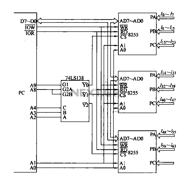
The computer control system is designed to detect signal path switching, requiring multiple input interface expansions. This system can switch all signal inputs into the computer. By utilizing a programmable chip, the 8255 expansion input interface allows for three...
There are two types of solar automatic tracking controllers. One type utilizes a Schmitt trigger light control, which consists of a light sensor and a Schmitt trigger or monostable trigger. The second type employs two light sensors and two...

The figure illustrates a simplified schematic diagram of the main circuit DMA12. It primarily consists of the input circuit, an electromagnetic interference (EMI) filter circuit, an impulse current limit circuit, an input rectifier filter circuit, a boost/power factor correction...

It is very convenient to automatically light a lamp in our absence during the evening when it gets dark. This automatic night lamp circuit can be utilized to illuminate staircase lights, porch lights, etc., automatically using a domestic power...
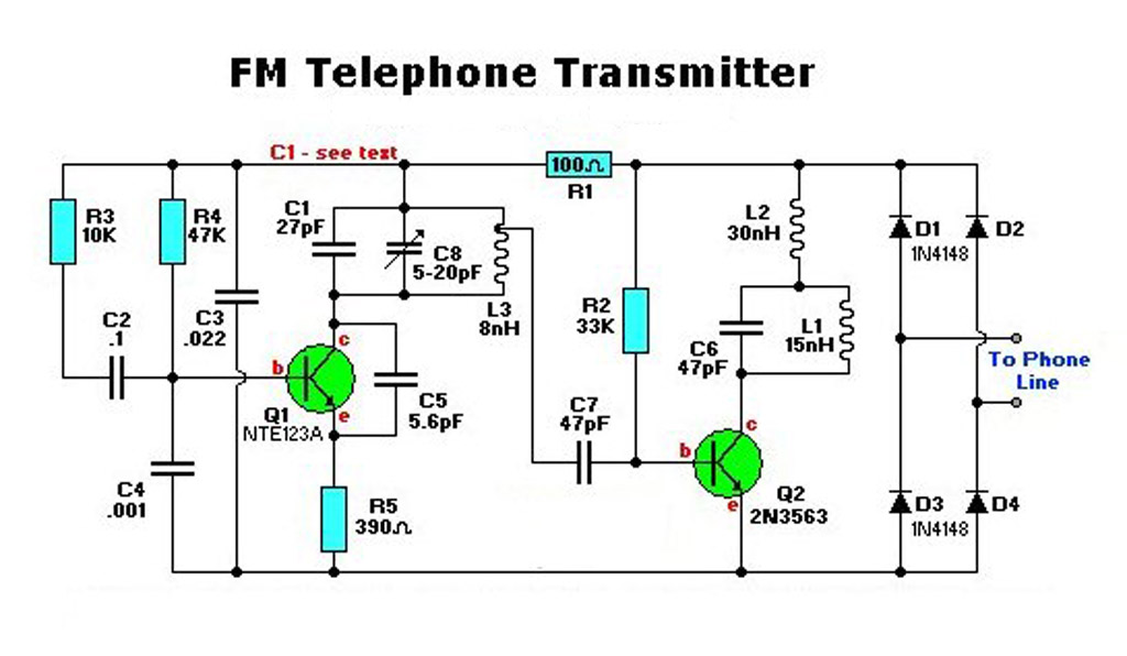
Electronic FM Telephone Transmitter Schematic. The following schematic design illustrates a circuit diagram for an FM telephone transmitter built on a compact PC board layout. This small design allows it to be easily integrated within the housing of a...
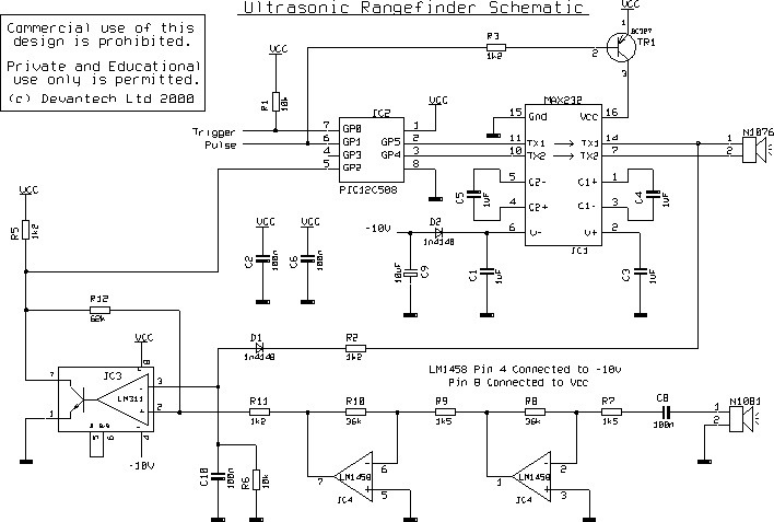
The following circuit illustrates an Ultrasonic Sensor Circuit Diagram. This circuit is based on the MAX232 IC. Features include a quiescent current of 150mA. The Ultrasonic Sensor Circuit utilizes the MAX232 integrated circuit, which is primarily designed for converting signals...