
ADA4858-3 used as a PIN diode driver circuit

The described circuit functions as a voltage level translator and signal conditioner, facilitating the integration of different logic families. The buffer gate at the input serves to isolate the input signal from subsequent stages, thereby preventing loading effects that could distort the signal integrity. The compatibility with TTL logic levels allows for seamless interfacing with various digital circuits.
The generation of a -1.5V reference voltage is crucial for applications that require bipolar signal swings, such as driving PIN diodes, which are commonly used in RF and photonic applications. The resistors R1, R2, and R3 are configured to establish this reference voltage by forming a voltage divider network. This network ensures that the output of the operational amplifier U1C accurately reflects the desired reference level while maintaining stability against variations in supply voltage.
The internal charge pump plays a pivotal role in generating the necessary negative voltage. By utilizing capacitors C3 and C4, the charge pump can effectively store and transfer charge, enabling the creation of the -1.5V output. The selection of these capacitors is critical; their values must be chosen to balance the charge transfer efficiency and the response time of the charge pump circuit.
In summary, this circuit design not only provides a robust solution for interfacing different logic levels but also ensures the proper operation of components like PIN diodes through the generation of a stable negative voltage reference. The careful selection of components and their configurations is essential to achieve optimal performance in various electronic applications.The figure can add a buffer gate at the input, so that the circuit compatible with TTL or other logic. This request is to TTL0V circuit to 3.5V input signal swing to a complementary -1.5V to + 3.5V swing for driving PIN diodes. R1, R2, R3 and U1C formed -1.5V reference voltage of the circuit, the internal negative voltage CPO produced by the internal charge pump. The charge pump capacitors C3 and C4 are necessary for the work.
Related Circuits
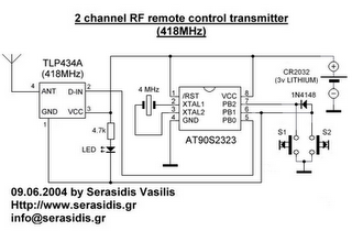
The following circuit illustrates a 3V power supply designed for an RF remote control circuit. This circuit is based on the AT90S2323 integrated circuit (IC). Features include a data rate of 2400 bps. The 3V power supply circuit for the...
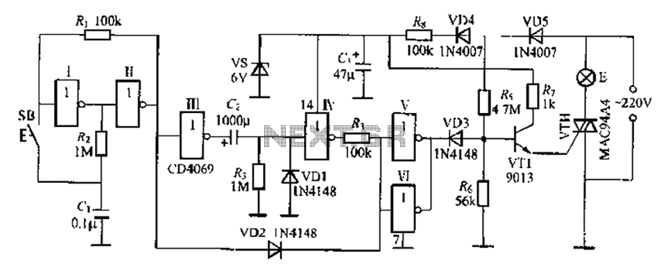
A delay lamp circuit is ideal for bedside tables, featuring a button (SB) that turns the light on and off. If the button is not pressed, the circuit maintains a delay before the light turns off. If the light...
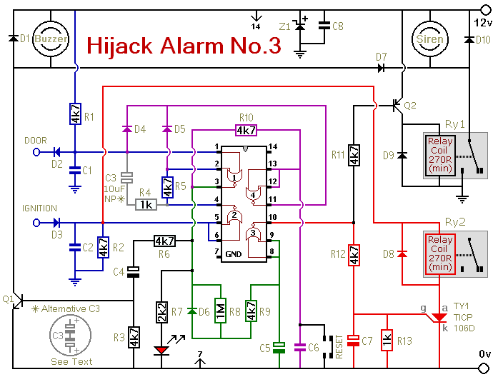
Similar to the initial two Hijack Alarms, this circuit is designed to activate if a door is opened while the ignition is switched on. After a delay of several minutes, allowing the thief to move a safe distance away,...
The metronome circuit has been assembled multiple times without success. Two manufacturers of the 555 timer, ON Semiconductor and National Semiconductor, provide circuit designs that differ from the original. In their designs, pins 2, 6, and 7 are not...
The circuit described here was designed as an addition to a remotely controlled garage door opener. The problem was that a brief burst of interference, arising from a thunderstorm or a mains spike, was enough to trigger the mechanism,...
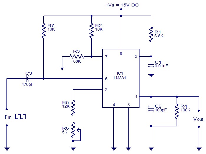
The following circuit illustrates a Frequency Voltage Converter Circuit. This circuit is based on the LM331 IC and operates with a supply voltage of 15V DC. The Frequency Voltage Converter Circuit utilizes the LM331 integrated circuit, which is designed for...