
Adding 1 PPS and 10MHz Outputs to the Z3801A
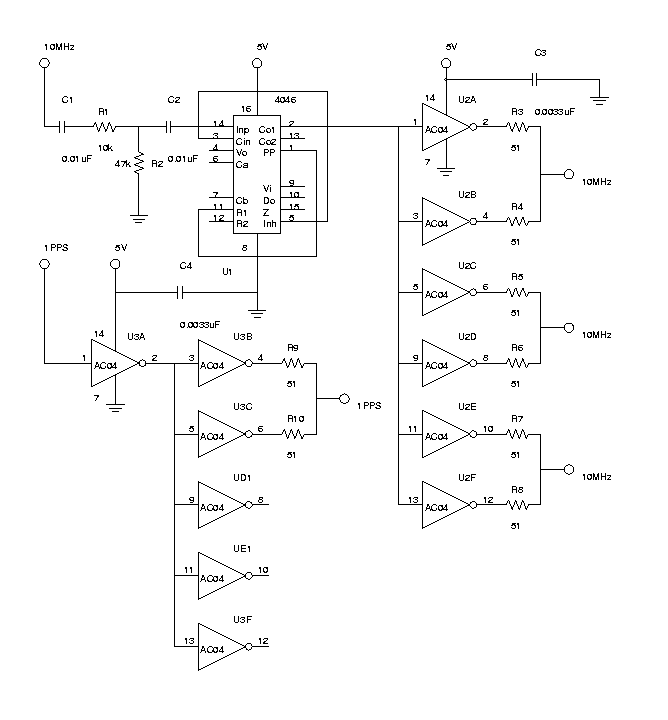
The Z3801A GPS-disciplined oscillator modification enhances its utility by providing both 1 PPS and 10 MHz outputs, facilitating its role as a reference clock for NTP servers. The design leverages existing signals within the oscillator, utilizing a combination of inverters and a phase-locked loop (PLL) to ensure reliable signal integrity. The choice of components, such as the 74AC04 inverter and 74AC4046 PLL, reflects a focus on speed and low jitter, critical for maintaining timing accuracy. The physical layout, with SMA connectors, allows for straightforward integration into existing systems while ensuring minimal signal degradation. The grounding strategy and power sourcing demonstrate practical considerations for circuit stability and reliability. This modification not only broadens the application scope of the Z3801A oscillator but also exemplifies effective circuit design principles in enhancing electronic systems.Make Z3801A GPS-disciplined oscillators more useful by making 1 PPS and additional 10MHz signals available on the rear panel, and providing a 1 PPS signal on the DCD line of the serial connector so the unit could serve as a reference clock for an NTP server. Although I ultimately want to add a distribution amplifier/splitter for the 10MHz sine wave signal, I thought it would be easier to initially add several
10MHz TTL square wave outputs. This page describes how I did that. Jeff Mock has published a modification that provides a nice RS-232 level 1 PPS signal on the DCD line, so I used that as the starting point. (Note: I`ve learned that Jeff`s web page is no longer there. A mirror is at. ) Jeff taps a 1 PPS TTL level signal off of U5, pin 2 (a Lucent 1141LL, whatever that is). I used that signal to drive my 1 PPS circuit. After probing around on the board, I was unable to discover a 10MHz TTL level square wave anywhere. However, TP5 in the front portion of the main board has a nice 10MHZ sine wave available, which unfortunately is riding on top of a DC bias voltage.
I used a piece of RG-174 cable to bring the signal from TP5 back to my circuit. The front pin of the adjacent TP4 complex is at ground, so I connected the RG-174 shield there. The 1 PPS circuit is very simple. I used a 74AC04 hex inverter, with the first section providing an initial inversion so that the end result remains a positive-going pulse. The output is a pair of inverters parallelled together through 51 ohm resistors; this combination provides a nice low-impedance signal that can drive a reasonable length of coax.
The unused sections of the 74AC04 must be tied to something; if they float, the chip may oscillate or otherwise find itself in a state of high current draw. I tied the unused inputs to the output of the first inverter, so they are available as additional 1 PPS signals if needed.
Since the 10MHz signal is a sine wave and I want to generate TTL square wave outputs, I struggled a bit with the best way to couple the signal into the digital circuitry. Finally, I settled on an idea used by Brooks Shera in his GPS-disciplined oscillator controller. Brooks used the input circuit of a 74HCT4046 PLL chip as an input conditioner. I wasn`t able to find the HCT version (and it`s not recommended for new designs, anyway), so I used a 74AC4046 instead.
The AC series part is faster and has lower jitter, so hopefully it will work at least as well in this application as the HCT version. My circuit has an added capacitor at the input that Brooks didn`t use; this keeps the input circuit from loading down the DC voltage on TP5.
I built the board on a piece of perf-board and mounted four SMA connectors on the rear panel for the new outputs. The board is supported by the short wires leading to the SMA connectors; this wouldn`t be wise if the unit were being banged around, but it should suffice for my application.
The board draws only a few milliamps at 5 volts, and I tapped power for it from the +5V test point on the power supply board. Ground is via a solder lug attached to one of the SMA chassis connectors. 🔗 External reference
Related Circuits
This circuit allows any infrared (IR) remote control to manage the outputs of a 4017 decade counter. It utilizes a 3-terminal IR receiver (IRD1) to capture infrared signals from the transmitter. The output from IRD1 is connected to an...
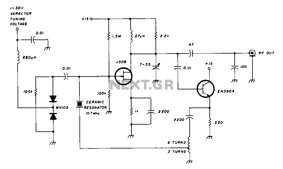
This circuit is an oscillator at frequency 10MHZ, using IC 1A and IC1B and a frequency divider. Using the IC2 it divides the pulses to 10. IC1C is a buffer. The variable capacitor 39pF is microtuning the frequency. The...

This section provides details for generating a composite video output signal from a camera to drive an external monitor. The circuit, designed by Peter Smith, integrates a DC-restorer, a switchable gamma corrector, and a video/sync mixer using a photodiode...
An extremely simple and low cost Sine/Square wave generator based on the Analog Devices AD9835 Direct Digital Synthesis (DDS) Generator chip. The frequency can be set for any frequency from 1Hz to 10MHz in 1Hz resolution steps! All this...
A field effect transistor amplifier features a fixed bias input source with feedback, resulting in very high input impedance and low capacitance. It drives a field effect transistor or emitter follower, despite having a very low output impedance, utilizing...
This tester is designed to locate stray electromagnetic (EM) fields. It can easily detect both audio and RF signals up to frequencies of around 100 kHz. However, it is important to note that this circuit is not a metal...
Warning: include(partials/cookie-banner.php): Failed to open stream: Permission denied in /var/www/html/nextgr/view-circuit.php on line 713
Warning: include(): Failed opening 'partials/cookie-banner.php' for inclusion (include_path='.:/usr/share/php') in /var/www/html/nextgr/view-circuit.php on line 713