
Alternately flashing lights chain multiple sets of high-power circuit 2

The circuit comprises three separate oscillators, each utilizing a transistor configuration to generate oscillations at designated frequencies. The transistors VTi, VT3, and VTs serve as the active elements in these oscillators, enabling signal amplification and frequency modulation. The oscillation frequency is primarily influenced by the resistive and capacitive components of the circuit, specifically Ri, R3, Rs, Cl, Cz, and C3s.
Resistors Ri, R3, and Rs are crucial in determining the time constants associated with the charging and discharging of the capacitors Cl, Cz, and C3s. The values of these components can be adjusted to achieve the desired oscillation frequency, allowing for precise tuning of each resonator.
The capacitors Cl, Cz, and C3s play a vital role in shaping the frequency response of the oscillators. Each capacitor interacts with its corresponding resistor to form a low-pass filter, which contributes to the stability and quality of the oscillation. The design of these resonators allows for a range of applications, including signal generation, modulation, and waveform shaping in various electronic systems.
In summary, the circuit's functionality hinges on the careful selection and arrangement of the transistors and RC components, enabling the creation of three independent multi-resonator oscillators with tunable frequency characteristics. By the transistor VTi, VT3 and VTs and RC components constitute three separate multi-resonator oscillator. Oscillation frequency levels dependent on the value Ri, R3, Rs and Cl , Cz, C3s.
Related Circuits
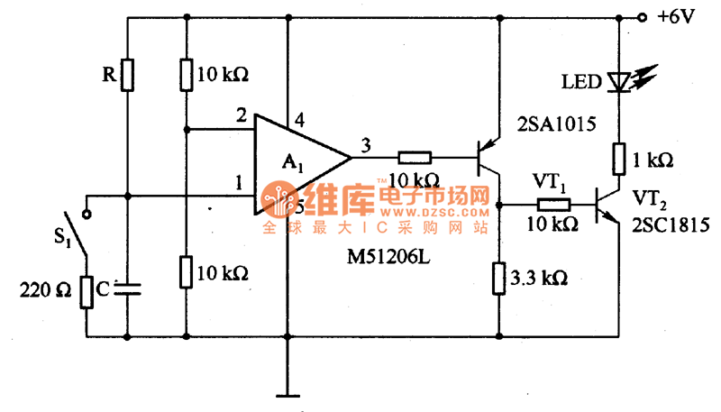
The circuit is designed to set a delay time based on the voltage Us and the resistor R. In this configuration, S1 acts as the discharge switch for capacitor C. When switch S1 is closed, the stored charge in...

The circuit utilizes a transistor (VT) and a voltage regulator (VSL) to create a constant current source, employing three regulators to enhance the performance of the regulator circuit. The described circuit employs a transistor (VT) in conjunction with a voltage...
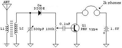
The following schematic illustrates a Crystal Radio Receiver Circuit Diagram that incorporates audio frequency (AF) amplification utilizing a Germanium transistor. The inclusion of AF amplification enhances the audio output quality. The Crystal Radio Receiver Circuit is a simple yet effective...
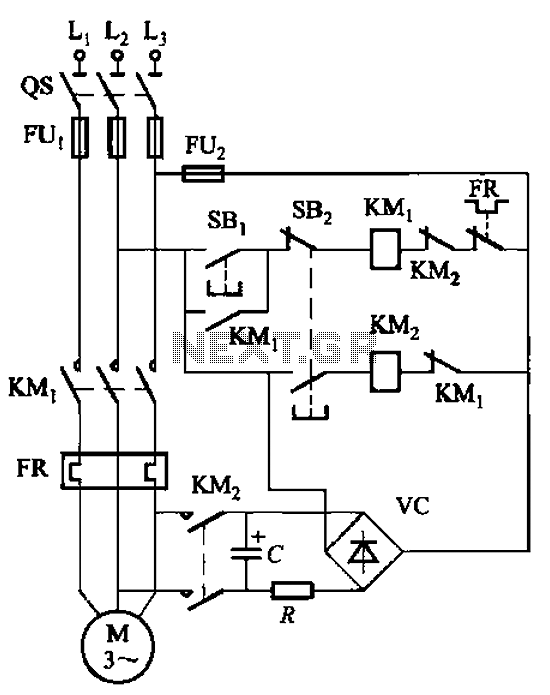
The circuit depicted in Figure 3-138 utilizes the principle of energy storage through capacitor discharge to achieve braking. The capacitance (C) and resistance (R) parameters are determined based on the size of the motor power. The capacitance (C) is...
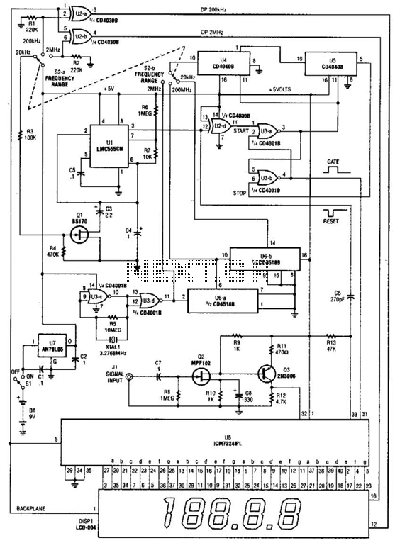
This is a schematic and block diagram of a 2-MHz frequency counter. It utilizes an LSI counter/display driver, an LCD readout, and several logic chips for timebase and timing pulse circuitry. Q2 and Q3 serve as a signal (input)...
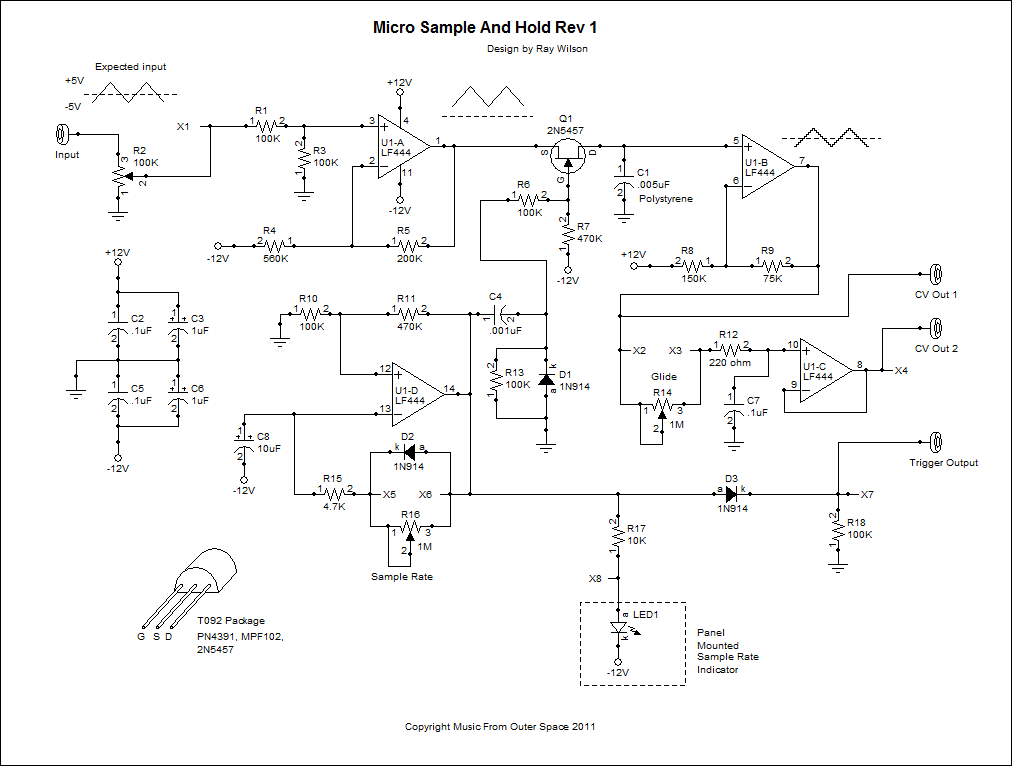
The voltage to be sampled is applied to the input of R2, a 100K linear taper potentiometer, while the other end of R2 is grounded. Consequently, the signal level that is sent to the buffering level shifter U1-A and...