
The time delay circuit diagram composed of transistor

The circuit operates by utilizing a timing mechanism that relies on the charging and discharging characteristics of capacitor C, influenced by the resistor R. The delay time is adjustable by varying the resistance value or the input voltage Us. When switch S1 is closed, capacitor C discharges rapidly, allowing the circuit to reset and prepare for the next timing cycle. The role of diodes VD1 and VD2 is crucial; they provide a path for reverse current, protecting sensitive components from voltage spikes that could arise during the discharge phase.
The timing circuit may include additional components such as a microcontroller or timer IC to enhance functionality, enabling more precise control over the delay intervals. The choice of resistor R and capacitor C values directly affects the time constant of the circuit, which is defined by the formula τ = R × C, where τ represents the time constant in seconds. This relationship allows for the calculation of the expected delay time, which can be fine-tuned based on the application requirements.
In practical applications, this circuit can be utilized in various timing-related tasks, such as in delay relays, pulse generators, or as part of more complex control systems in automation and robotics. Proper selection of components and careful layout design are essential to ensure reliable operation and to minimize noise and interference in the timing signal.It can set delay time according to the voltage Us and resistor R. In the circuit, S1 is the the discharge switch of capacitor C. When the switch S1 is closed, the stored charge on C will be released through S1 to ensure the accuracy of the delay time the next time. VD1 and VD2 are used to eliminate the impa.. 🔗 External reference
Related Circuits
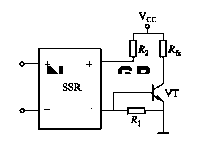
A DC solid-state relay (DC-SSR) driving a high-power load circuit is illustrated in diagram (a) below; the high-power load driving circuit is depicted in diagram (b) below. The DC solid-state relay (DC-SSR) serves as a crucial component in controlling high-power...
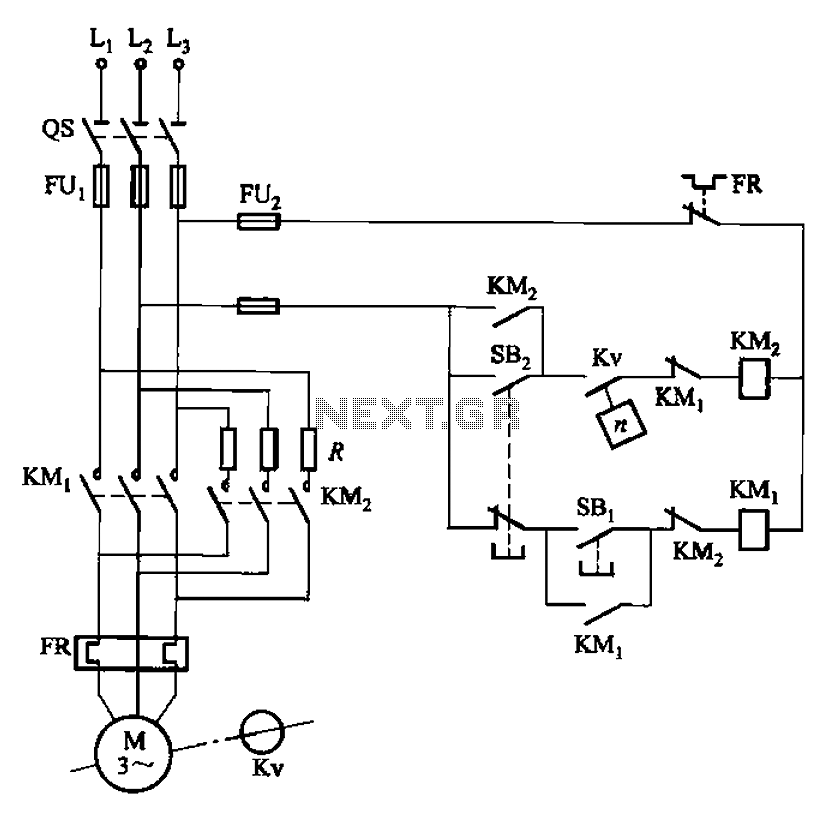
The circuit depicted in Figure 3-124 operates without an intermediate relay. Kv serves as the speed relay, activating when the electric motor speed exceeds 120 r/min while the contact is closed. If the speed drops below 100 r/min, the...
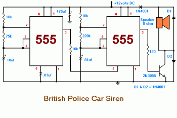
The 555 timer on the right is configured as an alarm sound generator, while the second 555 timer on the left functions as a 1 Hz astable multivibrator. The output from the left timer modulates the frequency of the...
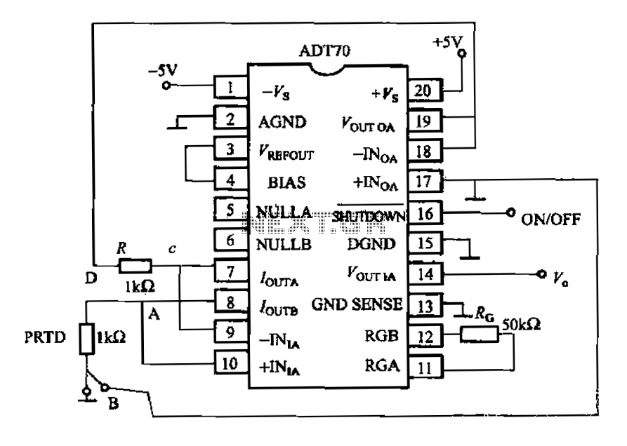
The AD170 basic electrical parameters include a temperature coefficient of 25 ppm/°C and a temperature measurement accuracy of ±1°C, with a maximum temperature range of -200°C to +100°C. The power supply required is +5V or -5V, and the operating...

This is an infrared-based broken beam alarm designed to protect doors and entry passages. It emits a loud alarm when someone crosses the invisible infrared barrier. The infrared-based broken beam alarm system operates by utilizing a pair of infrared emitters...

The circuit shown in Figure 3-21 is designed to produce a motor startup sound and a light signal indicating the completion of the startup process, after which the signal ceases. This circuit is tailored to control the motor for...