
An estimate of the load current monitor circuit rod

The circuit design involves multiple components working together to measure and display load current accurately. The operational amplifier serves as a key element, ensuring high input impedance and facilitating the voltage follower configuration, which minimizes loading effects on the circuit. The precision resistors (R3 and R4) are critical for maintaining measurement accuracy, and their low tolerance is essential for reliable performance.
The LM3914 display driver is configured to translate voltage drops into visual signals, allowing for easy monitoring of load current levels. The internal voltage divider that provides the 1.25V reference voltage is crucial for setting the thresholds for the comparators within the LM3914, ensuring accurate LED illumination corresponding to the measured current.
The filter capacitor (C3) plays a vital role in stabilizing the power supply to the operational amplifier, minimizing noise and fluctuations that could affect measurement accuracy. The choice of high-precision components and careful layout considerations contribute to the overall reliability and performance of the circuit.
In summary, this circuit design is suited for applications requiring precise measurement and display of load currents, with considerations for component selection, configuration, and power supply stability being paramount to its successful operation.Fig. A, b, c for the test rod end clip, a positive power supply terminating test equipment, b, c end series with the load, where c is the negative side of the device. Shu is th e sensing resistance measurements, loads of people because of its string loop, so it has a direct perception of the size of the load current. Since the product is less resistance, without affecting the load are functioning properly. Op amp IC. And BG composition suspension voltage follower, so flow through R, the load current is generated by the same pressure drop and the pressure drop on R3, Ding is flowing through the current and the voltage drop is proportional to Ri on R3, R4.
R5, R6 a current/voltage conversion ratio resistors R3 with its flowing through the same current, the resulting voltage drop that is on behalf of the table the size of the load current. Such as K 2 block is located, if the load current is 1A, then the pressure drop immediately to O.IV, also O.IV drop on R3, which the current imA, then the voltage drop across Rs is 1V, because this 2 block conversion ratio IV/a.
Similarly, the conversion ratio is 1 block 10V/A, 3-speed conversion ratio O.IV/A. Shaped display driver circuit consists of a linear ten point/line driver as the LM3914, IC, 7-pin output reference voltage of 1.25V, obtained from the RP IV sent an internal voltage divider as ten comparator reference voltage, while RP also determines the LEDl - LEDio operating current size, generally IF 1.25 x 10/RP. To make IC2 stable, filter capacitor C 3 is preferably close to the positive power supply pin. Fig 2 - 66 (a) of the resistor horse, R3, R4 Yun high precision, the general should be up to l% level.
If the load current is greater, Shu can take 0010, op amp Ic, should take the high input impedance type, such as CA3130, CA340, LF356, TL081 and the like. It is noteworthy that in Figure 2- 66 (a) applies only to the supply voltage +3 a 18V device estimate.
Figure 2 - 66 (Japan) also found that the current estimate of the display range Display resolution section of its tenth, and the load current increases, the more coarse resolution estimate results. To this end, FIG. 2 - 66 (a) may be employed in the right side of the broken line in Fig. 2 - 66 (b) bar-shaped display shown, this circuit is range resolution than Figure 2 - 66 (a) circuit is reduced by half.
Related Circuits
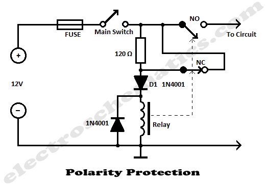
The simplest polarity protection technique is to connect a series diode to the power line input. The diode conducts only when the power supply is connected correctly. A series diode is an effective method for preventing reverse polarity in electronic...
A preferred STK4040xl Fi amplifier circuit exhibits excellent electrical parameters: under specific conditions, the output voltage (Uc) is 43V with a load resistance (RL) of 8 ohms. The circuit is designed to deliver a rated output power of at...
A 25kHz thyristor inverter welding machine circuit utilizes high-frequency operation to enable smaller transformer designs. The circuit diagram is illustrated in Figure 9-14. The no-load output voltage of the machine is 45V DC, with a peak voltage of 90V...
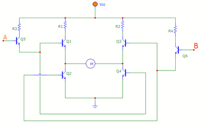
The transistors Q1, Q2, Q3, and Q4 form a bridge circuit. These are typically power transistors designed to handle high current. Transistors Q5 and Q6 drive the bridge. When input A is set high and input B is set...
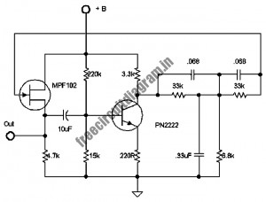
The following circuit illustrates a stable 60 Hz frequency signal generator circuit diagram. Features include a 0.068 µF capacitor incorporated within a feedback loop, allowing for DC-to-AC conversion. This circuit is designed to generate a stable 60 Hz sine wave...
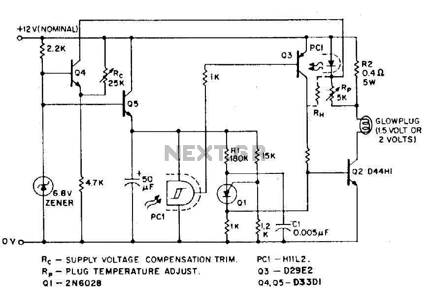
The circuit is designed for model airplanes, boats, and cars that utilize glow plugs for their miniature internal combustion engines (ranging from 0.1cc to 15cc). These engines are equipped with heavy batteries, high-tension coils, and capacitors necessary for classic...