
Antenna Combiner

The bottom side of the A3021B circuit reveals the four port amplifiers and the curving coplanar waveguides that transport the amplified antenna signals to the combiner. These amplifiers provide gain to counteract the loss introduced by the combiner itself. The combiner operates optimally when connected to a 50-ohm signal source, a condition that is consistently met by the amplifiers, regardless of their input terminations. By amplifying the antenna signal before it enters the combiner, the design maximizes the signal strength relative to the amplifier's thermal noise. The combiner introduces an attenuation of nearly 7 dB; therefore, positioning the amplifier prior to the combiner enhances the overall signal-to-noise ratio by 7 dB. The output attenuator ensures a stable impedance for both the antenna combiner and the cable, facilitating signal propagation to the A3018 amplifier input without causing reflections. With a 4-dB attenuator in place, the net gain from input to output of the combiner remains around 11 dB.
Testing of the A3021B's gain was conducted using a frequency sweep generated by a Modulating Transmitter (A3014MT). The frequency of the A3014MT was modulated using a triangle wave, with the output connected through a 1-meter RG-58C/U cable to the RF input of a ZAD11 mixer. The local oscillator input was sourced from an A3018C, and the intermediate frequency amplitude was measured with an oscilloscope at an RF frequency of 900 MHz. The ZAD11 exhibits an insertion loss of 7 dB, while the 1-meter RG-58C/U cable contributes an additional 0.7 dB loss, indicating that the A3014MT outputs approximately 4.8 dBm. The combiner's gain of 11.1 dB combined with the 6.6 dB insertion loss of the BP4C combiner and the added 1-meter cable loss results in a comprehensive assessment of the signal integrity.
The P1 amplifier delivers a gain of 22.4 dB, demonstrating the stability of the A3021B under various conditions. Attempts to induce oscillations through physical interference or by employing microwave absorbent foam, terminators, or rearranging cables yield no oscillations, affirming the circuit's unconditional stability. Notably, covering the microwave circuit with a hand results in a mere 5 dB reduction in gain, while the gain of P1 decreases to 10.5 dB when terminators are attached to the remaining three inputs. Even with all channels terminated, the minimum gain of the combiner remains at 10 dB, with the amplifiers providing a minimum of 21.3 dB at 900 MHz. The design and performance characteristics of the A3021 ensure robust signal amplification and reliable operation in its intended applications.The Antenna Combiner (A3021) is an active combiner for four 50- © coaxial antenna connections. The output is a combination of the four inputs with net gain of roughly +11 dB. The A3021 is intended for use with four Loop Antennas ( A3015B ), each of which is placed in a separate faraday enclosure and receiving signals from subcutaneous transmitters . The A3021 needs no terminators on its unused inputs. The circuit is unconditionally stable and isolates itself from local interference so effectively that it needs no shielding around the circuit board. We supply +5V power to the A3021 through a shielded LWDAQ Cable. Current consumption is 140 mA. We connect the other end of the cable to a LWDAQ Driver. The only purpose of the LWDAQ Cable is to provide +5V power. No communication occurs between the A3021 and the LWDAQ Driver. The A3021B is designed for use with the Data Receiver ( A3018 ). The A3018 is a LWDAQ Device, and so its presence assures us of a LWDAQ Driver into which we can plug the A3021.
The A3021 amplifies its four inputs, combines them, and passes the sum through an attenuator on its way to the output connector. The input ports are P1 through P4 on the schematic, and PORT1 through PORT4 on the circuit board. The output port is S on the schematic and SUM on the circuit board. Figure: The Bottom Side of the A3021B Circuit. We see the four port amplifiers and the curving coplanar wave-guides that carry the amplified antenna signals to the combiner.
The amplifiers provide gain to offset the loss introduced by the combiner. The combiner performs better when connected to a 50- © signal source, and the amplifiers always provide such a source, regardless of whether or not their own inputs are well-terminated. Furthermore, by amplifying the antenna signal before it passes through the combiner, we make sure the signal is as large as possible compared to our amplifier`s thermal noise.
The combiner attenuates the signal by almost 7 dB, so by placing the amplifier first, we improve our signal to noise ratio by 7 dB. The attenuator at the output of the combiner provides a well-behaved impedance for the antenna combiner and for the cable, so that the signal propagation to the A3018 amplifier input will be involve no reflections.
With a 4-dB attenuator on the combiner, the total gain from the input to the output of the combiner is around 11 dB. [05-JAN-11] We tested the gain of our first A3021B with the help of a frequency sweep provided by one of our Modulating Transmitters ( A3014MT ).
We sweep the frequency of the A3014MT with a triangle wave, as we describe here. We connect the A3014MT output through 1-m RG-58C/U cable to the RF (radio-frequency) input of a ZAD11 mixer. We obtain the LO (local-oscillator) input from an A3018C. We measure the IF (intermediate-frequency) amplitude with our oscilloscope for RF of 900 MHz and obtain the following table.
The ZAD11 has insertion loss 7 dB, and 1-m of RG-58C/U cable introduces a 0. 7 dB loss, so our A3014MT appears to be producing ’4. 8 dBm. The combiner amplifies by 11. 1 dB. The insertion loss of the BP4C combiner is 6. 6 dB at 900 MHz. We have a 4-dB attenuator in this particular A3021B. When we add the combiner, we also add another 1-m cable with 0. 7 dB loss. The P1 amplifier provides 22. 4 dB of gain. We cannot put the A3021B into oscillations with our hands, with microwave absorbent foam, with terminators, with unterminated cables, or by re-arrangements of cables. The circuit is unconditionally stable. Even when we put our palm on the entire microwave circuit, all that happens is the gain drops by 5 dB.
The gain of P1 drops from 11. 1 dB to 10. 5 dB when we add terminators to the other three inputs. The gain of the other channels is up to 0. 6 dB less than for P1. With terminators on all unused channels, the minimum gain of the combiner is 10 dB. The amplifiers provide at least 21. 3 dB at 900 MHz. The ERA-3SM data sh 🔗 External reference
Related Circuits
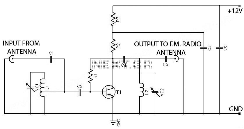
FM Booster, Active FM Antenna Amplifier. This FM booster can be used to listen to programs from distant FM stations clearly. The circuit comprises a common-emitter tuned RF preamplifier wired around VHF/UHF transistor 2SC2570. The FM booster circuit is designed...

The CYWUSB6953 is a comprehensive Radio System-on-Chip (SoC) device that facilitates the implementation of various simple RF systems using a single chip and a few discrete components. It is specifically designed for low-cost wireless systems that operate within the...
This 1 square meter antenna has radiation resistance of about 10 nanohoms, making the 0.4 Ohm resistance (including skin effect, which about doubled the resistance from the DC value) the dominant loss in the antenna. The lower the resistance,...
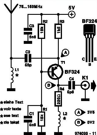
This inexpensive FM radio receiver antenna booster utilizes the BF324 TO92 style PNP transistor in a grounded-base configuration. The circuit can be employed as a... The FM radio receiver antenna booster circuit is designed to enhance the reception capabilities of...

This circuit is designed for a UHF TV antenna and provides a 15 dB preamplification. It is constructed using a transistor and minimal components. The schematic features the BF180 UHF transistor. The first stage consists of a band-pass filter...
All ATL-3 loop windings are centre tapped and balanced w.r.t. their amplifier/receiver chassis ground, and therefore electric field interference pick up tends to self cancel. Magnetic noise fields, e.g. televisions and the electric meter box, or electromagnetically radiated interferences,...