
Audio splitter amplifier circuit with TL084

The response is flat from 10 Hz to 30 kHz.
The described circuit utilizes a TL084 operational amplifier, which is a quad JFET-input op-amp, ideal for applications requiring low noise and high input impedance. The circuit is designed to amplify signals across three channels, making it suitable for audio applications or multi-sensor systems.
The initial stage employs capacitive coupling through a 1.0 µF electrolytic capacitor. This coupling method is essential for blocking any DC offset from the input signal while allowing AC signals to pass through. The choice of a 1.0 µF capacitor provides a suitable low-frequency cutoff, ensuring that frequencies down to 10 Hz can be amplified effectively.
The power supply configuration utilizes a single 9 V source, with the operational amplifier powered by a split supply of +4.5 V and -4.5 V (Vee Y2). This arrangement allows for symmetrical amplification, which is critical in audio applications to maintain signal integrity and minimize distortion.
The first stage of the amplifier achieves a voltage gain of 10, which is determined by the feedback resistor (1 MΩ) and the input resistor (100 kΩ). This gain is significant for boosting weak signals before further processing. The subsequent stages are configured as unity gain voltage followers, which serve to buffer the amplified signal without adding further gain. This configuration is advantageous as it provides high input impedance and low output impedance, allowing for effective signal transfer to the load.
Each output stage is coupled to a load through a 50 pF capacitor. This capacitor serves to isolate the output stage from the load, preventing any potential loading effects that could alter the performance of the amplifier. The load resistance of 5.1 kΩ is a typical value that balances power dissipation and signal integrity, ensuring that the output stage can drive the load efficiently.
The amplifier's frequency response is specified to be flat from 10 Hz to 30 kHz, indicating that the circuit is capable of handling a wide range of audio frequencies without significant attenuation or distortion. This characteristic is crucial for applications requiring accurate signal reproduction, such as in audio processing or instrumentation. Overall, the described amplifier circuit is well-suited for various applications where multi-channel signal amplification is required.The three-channel amplifier output distribution uses a single TL084. The first step is to capacitive coupling with a p. 1.0 ~ electrolytic capacitor. The entries are railways Vee Y2 or 4.5 V. This allows using a single 9 V power supply A voltage gain of 10 (1 M ohm ohm/l00 k) is obtained in the first stage, and the other three floors are connected as a unity gain voltage followers. Each output stage drives independently via an amplifier output 50 pF capacitor to the resistance of 5.1 k ohm load.
The response is flat from 10 Hz to 30 kHz.
Related Circuits

A 50-ohm impedance is illustrated in the RF2320 linear amplifier circuit, which is configured for input and output using transmission lines and inductive or capacitive components to create a matching network. The RF2320 linear amplifier circuit is designed to operate...
Almost all DC amplifier circuits are utilized as the input stage of differential circuits. Many complementary symmetry circuits also employ a double differential complementary sub-circuit along with a constant current source for the input stage. The constant current source...

This circuit is used to select modes of operation. The accelerometer is utilized to generally move the snake arm, while the Hall effect sensors are designed to enable various functions. The circuit described incorporates an accelerometer and Hall effect sensors...
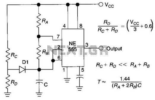
Using Rl, R7, and D1 to preset CI to one third of the supply voltage. This circuit avoids a longer first cycle period than subsequent cycles. The circuit described involves the use of resistors Rl and R7 along with diode...
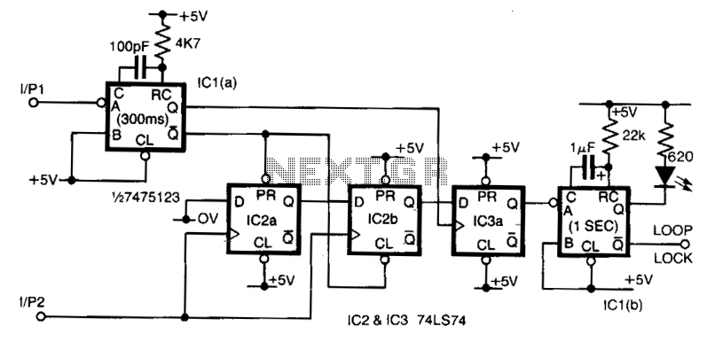
Input 1 functions as a gating period, during which a single rising edge on input 2 produces a logic 1 output. Any other input that indicates non-identical frequencies results in a logic 0 output. IC1a converts input 1 into...
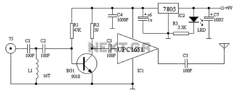
Circuit Overview Many families now own various electronic devices such as televisions, VCD players, video recorders, game consoles, cameras, and DVDs. This circuit involves an RF signal repeater designed to work with a television signal transmitter, covering a radius...