
Auto Fade Implementation on Audio Signals Project PCB

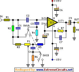
The TL072 operational amplifier is designed for low-noise applications and features a JFET input stage that provides high input impedance. This characteristic minimizes loading effects on preceding stages and allows for accurate signal amplification. The operational amplifier's high slew rate enables it to handle rapid changes in input signals, making it suitable for audio applications where dynamic range is essential.
The 4011 NAND gate integrated circuit provides logical operations essential for digital signal processing within the circuit. Its ability to drive multiple inputs ensures that the circuit can be expanded or integrated with other digital components without compromising performance.
The 4066 analog switch allows for the selective routing of signals, providing flexibility in managing audio paths. Its low ON resistance contributes to minimal signal loss, ensuring high fidelity in audio applications.
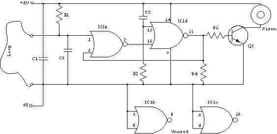
The signal processing chain begins with the microphone, where the initial sound input is amplified by IC1A. The gain is adjustable via RV1, allowing for optimization based on the input sound level. The interaction between the potentiometer and IC3 ensures that the signal is processed effectively, with the switches enabling or disabling the signal path based on the presence of audio excitation.
The rectification stage involving D1 and D2 is critical for converting the AC audio signal into a DC format suitable for further processing. This DC signal is then used to control the operation of IC2A and IC2B, enabling dynamic response to the audio input.
The circuit's design allows for seamless switching between stereo channels, ensuring that audio signals are maintained without distortion. By testing the circuit with a musical input, it can be verified that the outputs maintain the integrity of the sound, confirming the effectiveness of the design.
In summary, this circuit integrates analog and digital components to create a robust audio processing solution that is adaptable for various applications, maintaining high performance and fidelity throughout its operation.TL072 a low noise JFET input operational amplifier with features such as common-mode input voltage range, high slew rate, operation without latch up, compensated internal frequency, high input impedance at the JFET input stage, low noise, low total harmonic distortion, protected from output short circuit, low input bias and offset currents, wi de common-mode and differential voltage ranges, and low power consumption * 4011 a quad 2-input NAND gate integrated circuit, generally characterized by small fluctuation in voltage supply, very high impedance, outputs that can sink and source, one output can drive up to 50 inputs, high speed gate propagation time, high frequency, and low power consumption * 4066 a digitally controlled quad analog switch utilizing advanced silicon-gate CMOS technology with features such as individual switch controls, matched switch characteristics, pin and function compatibility, low quiescent current, low ON resistance, wide analog input voltage range, and 15 ns typical switch enable time The operation of the circuit is built about the function of amplifier IC1A that strengthens the signal of microphone by regulating the gain of the unit depending on the needs. The intensity of the sound is adjusted by the potentiometer RV1, which is fed via pins 9 & 10 to the two switches of IC3.
The switches are possessing resistance of 10M ohms when no excitation is present while a resistance drop to 300 ohms occurs during excitation which allows the signal to pass through. When the signal reaches a specified level, due to additional strengthening of IC2B via RV2, it will be rectified by D1 & D2.
An interrupted DC signal is produced by the circuit in the pattern of IN1 signal and this is being used to change the operation of IC2A and IC2B. The stereo signal can pass when IC3A and IC3B are turned ON. When the input of J1 contains audio excitation, the operation of IS2A & IS2B will change that affects the state of IC3, causing the switch A-B to open and C-D to close.
The stereo signal is interrupted and allowed to flow from the input of J1. The circuit can be tested by using placing a musical program in the input of J2 & J3, which passes to the outputs of J4 & J5, without distortion or reduction of signal for the two channels. The use of capacitor C5 is to pass the signal of microphone when the signal reaches a certain point. The circuit will vibrate as the speech is done. 🔗 External reference
Related Circuits
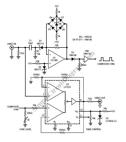
Fading a video signal cannot be achieved merely by attenuating the composite signal, as the synchronization signal may fall below an unacceptable level. Fading a video signal involves a careful adjustment of both the luminance and chrominance components while...
Is there an amplifier located in your living room, basement, or home theater that you would like to activate when music playback begins? To achieve the desired functionality of automatically turning on an amplifier when music is played, a simple...
To achieve optimal audio reproduction at varying listening levels, it is essential to adjust tone control settings to align with the established characteristics of human auditory perception. The sensitivity of the human ear changes non-linearly across the entire audible...
The loop can be any type of hookup wire, with a maximum resistance of about 90K. Using very thin wire (40AWG, for example) will create a highly sensitive trip wire, but will reduce the distance it can be strung...
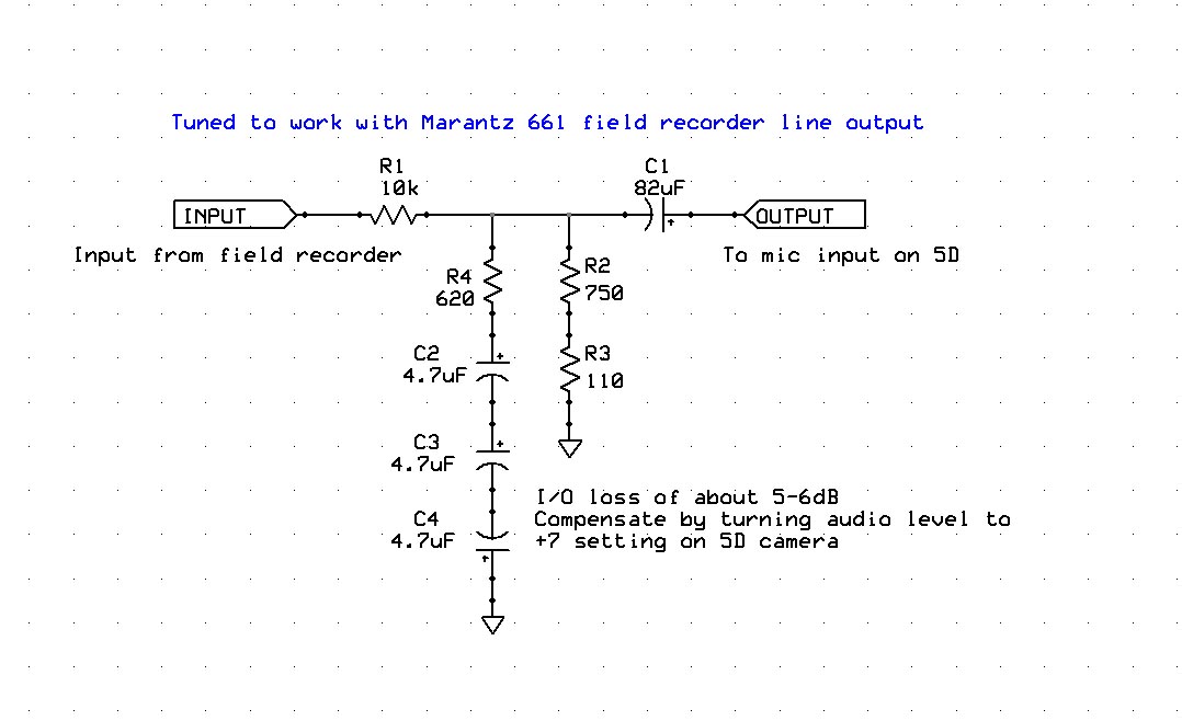
Enhancing the audio quality of the Canon 5D Mark II to achieve usable production audio involves several key steps. The initial phase of this engineering project focuses on data collection, specifically measuring the input frequency response of the 5D....
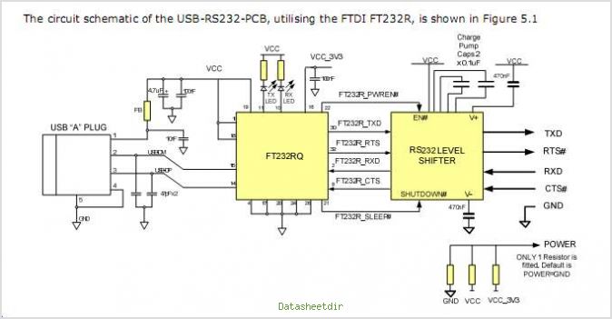
The USB-RS422-PCB is a printed circuit board (PCB) designed as a USB to RS422 level serial UART converter. It utilizes FTDI's FT232RQ USB to Serial UART Interface IC, which manages all USB signaling and protocols. This PCB offers a...