
Auto Turn-Off Alarm With 8-Minute Delay

The circuit design incorporates a NE555 timer configured in astable mode to produce a continuous square wave output. This output serves as the clock signal for the CD4020B binary counter, which is a 14-stage ripple counter capable of counting up to 16384. The pulse frequency generated by the NE555 timer can be adjusted through the selection of external resistors and capacitors connected to its timing pins.
When the circuit is powered with a +12 Vdc supply, the timing capacitor C2 initially charges, causing the output of the CD4020B (IC2) to be low. This low output state activates a relay, allowing current to flow through the relay coil, which in turn can control a larger load. The NE555 timer (IC1) produces a series of pulses that increment the count in the CD4020B. Each pulse corresponds to a clock cycle, and after 8192 pulses, the output at pin 3 of IC2 transitions to a high state.
This transition from low to high at pin 3 of the CD4020B serves as a control signal that turns off transistor Q2, thereby deactivating the relay. The relay's deactivation may be used to switch off a load or to signal the completion of a specific operation. The overall design allows for precise timing and control, making it suitable for applications where sequential operations are required based on a defined count or timing interval.
Proper selection of components, including the NE555 timer's resistors and capacitors, as well as the relay specifications, is crucial for ensuring reliable operation and desired performance characteristics of the circuit. This circuit uses a NE555 timer and CD4020B. When +12 Vdc is applied to the circuit, the output of IC2 is set low via C2, which turns on the relay, and IC1, a pulse generator. IC1 pulses counter IC2. After 8192 clocks, IC2 output (pin 3) goes high, cuts off Q2, and completes the cycle.
Related Circuits
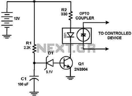
This circuit design was used to switch on device via a LED photocell arrangement (optocoupler) using components R1, C1, D1 and Q1. It produces a delay on powering up to ensure correct sequencing of certain equipment. A very simple...
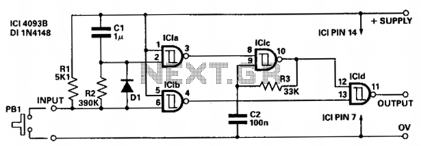
The circuit provides independent control of the initial delay and pulse rate. ICIc functions as a pulse generator, with its operation inhibited by the normally low output of ICla. When the circuit input transitions to low (e.g., when pressing...
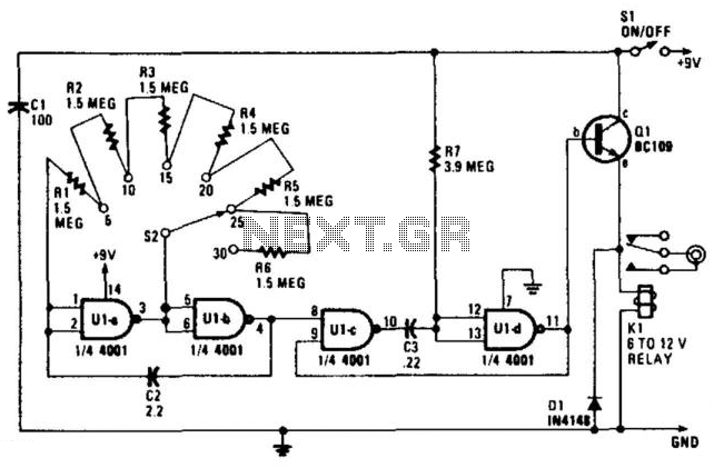
A 4001 CMOS Quad NOR gate is configured as an astable multivibrator, which drives a simple differentiator and relay driver. Depending on the setting of S2, a delay of 5 to 30 seconds is generated. S2 and R1 through...
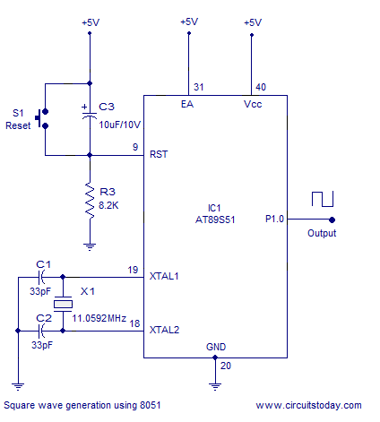
A software delay routine in the 8051 microcontroller is utilized to generate various time delays. This project features a sine wave generator circuit that employs a software delay within the 8051 architecture. The AT89C51 microcontroller serves as the core...
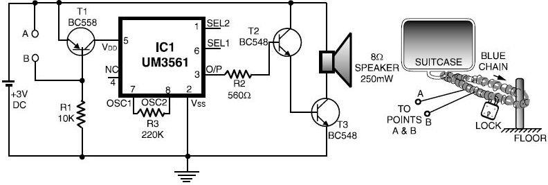
This luggage or bike alarm can be utilized while traveling by train or bus. Typically, luggage is secured using a chain-and-lock arrangement; however, there are still vulnerabilities. The luggage or bike alarm system is designed to enhance the security of...
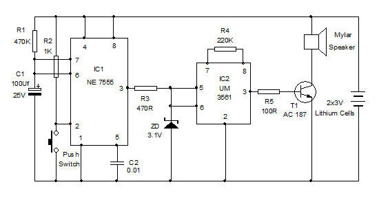
Personal Alarm Circuit Diagram. If you feel threatened or need urgent support in a crowd, use this alarm to catch the attention of others. The personal alarm circuit is designed to provide a loud audible signal when activated, serving as...