
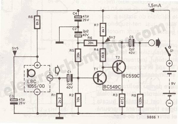
Automatic telephone answering circuit diagram

The automatic telephone responder circuit is designed for seamless operation in response to incoming calls. The core components include an electret microphone for sound capture, a voice recording IC (SR9G10A) for storing the audio message, and a relay system to simulate an off-hook condition.
Upon receiving a call, the circuit employs an optocoupler (4N35) to detect the ringing signal. This detection is crucial as it triggers the playback of the recorded message stored in the voice recording IC. The audio signal is processed through a series of transistors, specifically VT1 and VT2, which modulate the voltage levels necessary for activating the relay (J1). The relay acts as a switch that connects the telephone line to the playback system, allowing the caller to hear the pre-recorded message.
The use of a static triode (VT1) ensures that the circuit remains inactive until a call is detected, minimizing power consumption. The voltage levels are carefully managed to ensure that the transistors operate efficiently, with the VCE of VT2 being a critical threshold for activating the relay. The diode (VD2) and transistor (VT3) configuration is essential for ensuring that the relay is only activated during the playback phase, preventing any unintended connections to the telephone line.
Once the message has been played, the circuit automatically resets, releasing the relay and returning to a standby state, ready for the next incoming call. This design provides an effective solution for automatic telephone responses, allowing users to communicate effectively even when they are unavailable to answer calls directly. The circuit can be further enhanced with additional features such as adjustable recording time, volume control, or integration with digital storage for improved message quality. Automatic telephone responder circuit is shown in Fig. FIG IC2 10 seconds voice recording circuit SR9G10A, press the power switch S2, can be built by IC2 electret microphone in put if you want to tell a friend. Before going out to press the switch Sl, static triode VTl, composite pipe collector voltage VCE VT2 composed of about 0.65V, diode VD2, transistor VT3 nonconductive.When a call hit, the phone ringing, ringing signal negative half-cycle so that ICl 4N35 optocoupler conduction, IC2 of PLAYE grounded (equivalent to a falling edge of the negative pulse trigger) while playback, the audio signal all the way to unilateral after the composite tube amplification, the transistor VT2 of VCE increases, VD2, VT3 turn, relay Jl pull, the resistance Rl analog outside line off-hook (telephone DC resistance of about 300 ); another unilateral way audio signals added to both ends of the telephone line, so your friends hear your voice input in advance. When the sound after sowing, the circuit back to the static relay J1 release, the entire state of the circuit corresponds to hang up.
Related Circuits

This field strength meter consists of a tuned crystal detector that generates a DC output voltage from a transmitted signal. The DC voltage is utilized to modulate the frequency of a transmitter with a power output of 100 mW,...
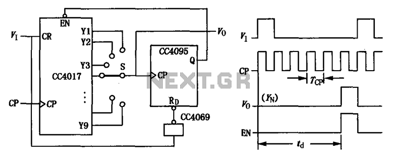
CC4017 counter/distributor featuring a circuit diagram of the delay. The CC4017 is a decade counter and distributor that counts from 0 to 10, providing ten output states. It is commonly used in various digital applications for counting purposes, such as...
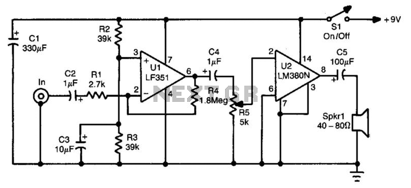
This amplifier is suitable for telephone applications or situations where a straightforward speech amplifier is necessary. The frequency response can be adjusted by changing the values of capacitors C2 and C4, and by adding a capacitor across resistor R4...
This audio amplifier circuit is designed for use in classrooms to alleviate the strain of lecturing in noisy environments. It incorporates the power amplifier IC LM380, which delivers an output of 2 watts, adequate for confined spaces. The amplifier...

Figure 1 illustrates a circuit that utilizes a single +V power supply and a voltage output Digital-to-Analog Converter (DAC) known as the AD5620. The DAC is controlled via an SPI port, with its output ranging from 0 V to...

This is a simple circuit that functions as a tachometer. It operates as a frequency-to-current converter, transforming the incoming signal into a proportional current to drive the meter. The deflection on the ammeter correlates directly with the frequency of...