
Charging capacitor bank with current limiting circuit

The current limiting circuit operates by using a sense resistor (R_sense) to monitor the current flowing through the load. The op-amp compares the voltage across R_sense with a reference voltage to maintain the desired current limit. When the load attempts to draw more than 480 mA, the op-amp adjusts the gate voltage of the MOSFET, thereby reducing the current flowing to the load. This feedback mechanism ensures that the current remains within safe limits, protecting both the circuit components and the power supply.
In applications involving the charging of a capacitor bank, the challenge arises from the instantaneous current draw when the capacitor is connected. To avoid damaging the power supply, it is essential to implement a method to control the charging current. One approach is to pre-charge the capacitor to a known voltage before connecting it to the circuit, which can be achieved through a controlled switching mechanism. Alternatively, using a P-channel MOSFET allows for high-side switching, providing better control over the current flowing into the capacitor bank.
It is important to consider the characteristics of the capacitors used in the design. The equivalent series resistance (ESR) and capacitance value will affect the charging dynamics. During the charging process, the current will initially be high, but as the capacitor voltage approaches the supply voltage, the current will decrease. This behavior can be modeled in simulation software, but care must be taken to include realistic component values and initial conditions to ensure accurate results.
In summary, the current limiting circuit is a vital component for protecting electronic systems from excessive current draw, especially in scenarios involving capacitive loads. Proper design and simulation techniques are essential for achieving the desired performance and ensuring the reliability of the circuit in practical applications.A useful current limiting circuit (shown below), that allows me to select a maximum current through a load. The circuit is set to give a 480 mA max current. As the load resistance increases, the SER of the limiting circuit drops away. The following plot shows current through the load versus load resistance. . . However, what happens if I want to charge a capacitor bank using this circuit. Where would I put it Current needs to flow through R_sense to cause a voltage drop in order for the circuit to function. If I just add a capacitor after the sense resistor. . . Then the voltage of the cap jumps up to 4. 8 volts immediately (which I`m guessing would draw a massive current, fry my supply, and negate the point of the current limiting circuit) This looks pretty logical to me.
If a cap is connected to an ideal voltage source, it will get an infinite current and be at 4. 8 V instantaneously. What do I need to do in order to reproduce the effect shown in Oli`s lowest plot For the second simulation with the cap at the top, you need to set the cap voltage to 0V initially. I did this by setting the voltage at the MOSFET drain to 4. 8V, the. ic V(n001) 4. 8 you can see next to the cap is the SPICE command to do this. This means both ends of the cap are at 4. 8V hence there is no voltage across it. I`m not sure how you do this in Circuit Lab, if you can link to your circuit maybe I (or someone else more familiar with it) can help.
Oli Glaser Sep 5 `12 at 13:03 Okay, thanks. Unfortunately it seems there is no way to do this in CircuitLab yet. They suggest using a time controlled switch switching at T=0 as a workaround. CircuitLab is pretty, but it`s not as sophisticated as SPICE - if you are planning on doing plenty of EE, then I`d advise getting to know SPICE (LTSpice is a great free version from LT, there are also other options like NI Multisim, TINA from TI, ngspice, etc) Oli Glaser Sep 5 `12 at 13:27 Wow, thanks for the help Oli! So the current limiter in this case is controlling the discharge rate of the -ve plate. I eventually want to place a load across the cap that might spike huge current (hence the big cap). Would I be better modifying this circuit to us a Pch MOSFET and use high-side limiting It is the supply that I want to protect, not the load.
learnvst Sep 5 `12 at 14:49 The opamp is trying to keep the voltages on it`s inverting input the same as the non-inverting input, which is 240mV in your example above. To do this with just Rsense present, it must keep 480mA flowing through Rsense as you say. Now, with the cap in series, it will actually work to charge the capacitor as you have it. However, the catch is that it will not be at a constant current, and the cap will only charge to 240mV, since this it what the opamp needs to keep the balance.
The cap does not pass DC, so the current is initially 480mA, and drops exponentially down to 0 as the voltage rises (and the voltage across the resistor drops) Another thing to understand here is that a simulation is only as real as you make it, and in some cases the ideal components cause problems. It`s quite common for the simulator not to converge or produce odd results if there is no DC path available.
Also with a transient simulation, you sometimes need initial conditions set to observe a process. For example, if I simulate the above circuit in LTSpice with an ideal 1F capacitor, the simulation does not converge (never finishes) If I add a high value of parallel resistance (10M ©, this is actually very conservative for such a large value, probably be much lower) to provide a DC path, and (very roughly) simulate real world imperfect capacitor leakage, the simulation works: The 240mV is produced by the 24nA across the 10M © res 🔗 External reference
Related Circuits

The following circuit is a power amplifier circuit for an FM transmitter with an output power of 30 watts. The power amplifier circuit utilizes a power transistor of type 2SC1946A. The FM transmitter operates with a 13.8-volt DC power...
The UC3842, UC3843, UC3844, and UC3845 series of oscillators can generate synchronization pulses without requiring numerous external components. The following circuit illustrates the Sync Pulse Generator Circuit Diagram for the UC3842/3/4/5. This sync pulse circuitry is capable of operating...
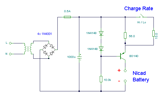
This simple charger utilizes a single transistor as a constant current source. The voltage across the pair of 1N4148 diodes biases the base of the BD140 medium power transistor. The circuit operates by employing the BD140 transistor to regulate the charging...
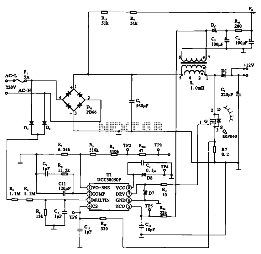
A typical laptop power adapter circuit converts an AC input of 22V through a rectifier and filter circuit to produce an output of +30V DC. This voltage is then processed by a switch oscillation circuit (U1, UCC38050P), which controls...
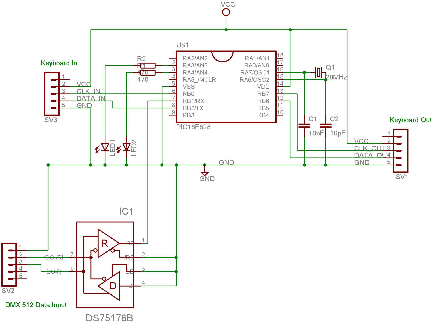
This system is designed for use with a PC connected to video projectors, enabling a lighting controller to manage a presentation displayed on the video screen. The PC used for the presentation is situated in a different location from...
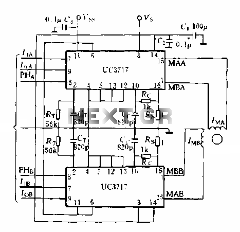
A typical application of a two-phase stepper motor is illustrated in Figure 5-15. It consists of two UC3717A components that can create a microcomputer control system for a two-phase permanent magnet or hybrid stepping motor. The control signals for...