
Cheap Switch-Mode DC-DC Converter

The circuit operates as a step-up (boost) converter, leveraging the MC34063, which is designed for efficient voltage regulation. The key components include the MC34063 IC, an inductor, a diode, and the feedback resistors R1 and R2. The inductor stores energy during the ON phase of the switch, while the diode allows current to flow to the output during the OFF phase, effectively increasing the voltage.
To achieve the desired output voltage, it is essential to select appropriate resistor values for R1 and R2. The feedback network formed by these resistors sets the regulation point of the output voltage. For instance, if R1 is set to 100 ohms and R2 is set to 300 ohms, the output voltage can be calculated as follows:
Vout = 1.25 (1 + 300/100) = 1.25 (1 + 3) = 1.25 * 4 = 5V.
This flexibility allows for a wide range of output voltages, making the circuit suitable for powering various devices requiring different voltage levels.
In addition to the resistors, the selection of the inductor is critical, as it must be rated for the desired output current and voltage. The diode should be a Schottky type to ensure minimal voltage drop and faster switching speeds. Proper bypass capacitors should be included at the input and output to filter out any noise and stabilize the voltage levels.
Overall, this circuit design is efficient and versatile, making it ideal for applications in portable electronics where space and power efficiency are paramount. Proper layout considerations should be taken into account to minimize parasitic inductance and resistance, which can affect performance.This circuit is based on mobile phone chargers. These chargers are based on the Motorola MC34063 switchmode IC. By changing the values of the feedback resistors (R1 & R2), the output voltage can be varied over a wide range. Just modify R1 and R2 according to the formula: Vout = 1. 25 (1+R2/R1). The values shown give an output of 3V. 🔗 External reference
Related Circuits
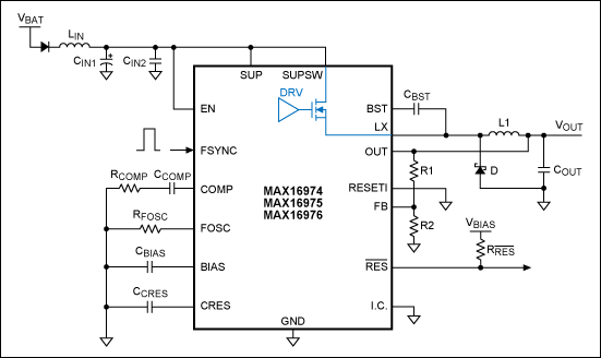
Optimize the layout of the MAX16974/MAX16975/MAX16976 high-performance DC-DC converters, which are standard buck controllers designed for automotive applications. The MAX16974, MAX16975, and MAX16976 are advanced DC-DC buck converters specifically tailored for automotive environments. These devices are engineered to deliver high...
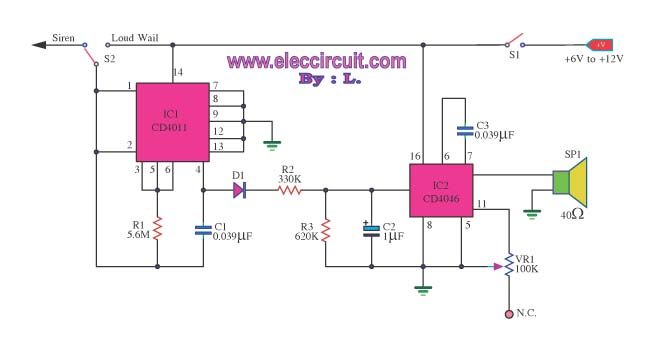
This is a siren sound generator circuit that is cost-effective and capable of producing simple sound patterns. The circuit utilizes IC1, which is a CD4011 (Digital NAND Gate), and IC2 is... The siren sound generator circuit is designed to produce...

The 24V to 12V converter schematic is straightforward; however, it is important to ensure that all components, including transistors and integrated circuits, are adequately heat dissipated and electrically insulated from metal surfaces. The schematic diagram is derived from the...
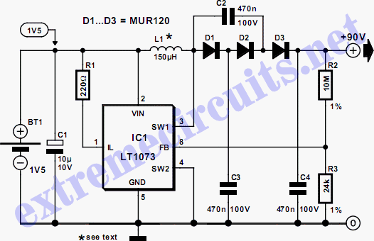
The circuit illustrates a method to obtain a voltage of 90V from a 1.5V battery supply. The LT1073 switching regulator from Linear Technology operates in boost mode and can function with an input voltage as low as 1.0V. The...
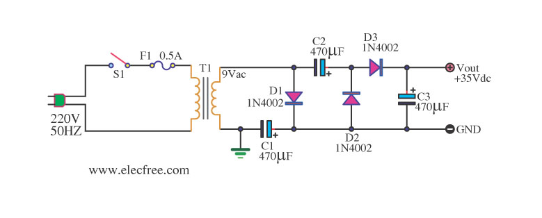
Simple AC to DC converter 9VAC to 35VDC. This is a basic example of an AC to DC converter model designed to be straightforward. It modifies 9VAC input to produce 35VDC output, depending on various factors. The AC to DC...
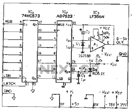
The IC latch is utilized to hold the digital data when the clock signal rises. The configuration includes a holding data port AD7s23, a thin film resistor ladder, and a switch that together form an 8-bit Digital-to-Analog Converter (DAC)....