
Build your own simple IC tester applied to standard TTL or CMOS IC

This electronic project centers around the design and implementation of a simple integrated circuit (IC) tester that evaluates various ICs using the PPI-8255 programmable peripheral interface. The circuit utilizes a parallel port for communication, which is essential for bi-directional data transfer. The PPI-8255 is a versatile chip that provides three 8-bit ports, enabling interaction with the IC under test. Port-A is designated for sending logic states, Port-B for reading logic states, and Port-C for controlling the enabling functions of latches and buffers.
The operational design ensures that the device can automatically select pin power through relay devices, enhancing usability. The inclusion of a truth table for the PPI-8255 clarifies the expected outcomes for various input combinations, ensuring proper functionality during testing. The double-sided PCB design allows for compact integration of components, although manual jumpers are necessary for connections due to the limitations of the fabrication process.
In terms of construction, attention to detail is critical to prevent short circuits between the ground and Vcc. The use of IC sockets is recommended to facilitate easy replacement, thus minimizing downtime and enhancing the reliability of the testing process. The project exemplifies a practical approach to digital circuit testing, providing a valuable tool for engineers and hobbyists alike. The software component, originally developed in Quick Basic, is intended to evolve into a more robust application potentially utilizing Delphi for improved user interface capabilities on Windows platforms. This transition aims to enhance the overall user experience while maintaining compatibility with the underlying hardware architecture.What is mean logic-1 or logic-0 Logic-1 and logic-0 strongly connection between the state at one moment and one condition. Logic-1 means any states are in the condition of high voltage close to Vcc voltage, and logic-0 means any states that close to netral or ground voltage.
Is that just right that. What about logic philosophy Logic philosophy are like this, at one state, logic-0 cannot be made to be come logic-1 but logic-1 can be made to be logic-0. So if we want to exam the output of any devices (like and gate, or gate, not gate, buffer, counter, etc.
), the output logic must be keep to be logic-1, then the input logic can be applied and the output logic will be changed by the result. This project was dedicated to Paul Stenning at where the idea come when I saw his project. The project used a standard serial port type. I got quiet difficult to find this type IC. So I made the parallel port version. The concept is still the same. I changed only the part of serial to parallel convertion data. But my program still can used both hardware, serial port type or parallel port version. Certainly I didn`t try the serial version, because I didn`t build it, so if someone have found any bugs, please report it to me.
I will fix it. Thanks to Paul because of his great thinking. I myself already tried a long time ago to make a device like this (simple ic-tester) to test any other ICs in my junk trash can. Thank you very much Paul`S ! Some part was changed to accomodate the parallel type port. The original clock circuit, RS-232 buffers and interface was omitted and replace with the parallel port interface and the flip-flop latch changed with 8-bit latch, so the circuit is more simpler.
Other parts are still the same accept that the selector switch to select the IC power was changed to relay devices. So we can make the device a little automatic selecting pin power. The device must used bi-directional LPT parallel port (because the standard LPT parallel port can not accomodate the data interchange).
All control signals are used to make the combination of control function for PPI-8255. More about explanation for this IC type can be seen at another topic, LPT extender and expander ). This IC configured for port-A as output port, port-B as input port and port-C as output port. Port-A used to send logic state to IC under test, port-B used to read logic state from IC under test and port-C used for input decoder to select the enable function of latches and buffers of IC under test and also to activated the relay power circuits. Tabel I-1. shows the functional truth table for operational of this PPI-8255 for our purpose. I already built this prototype by using double sided PCB using protel software design. The design was still crowded, but it worked. Many jumper must be made to both sides, because we didn`t have a fabricate one ( this create manually ).
I used a tiny email wire (or you may use wire from nyy cable). Even its already double layer, it needs also many jumper, so don`t forget to put it in the right way. Note that the common copper clad of top layer is ground and the common copper clad of bottom layer is Vcc.
Don`t forget to test it with ohm tester (bell check). this copper side both layer must not short circuited. Also Vcc and ground for any IC must be checked there were connected or not. Its better if we used many socket for ICs, because if any IC known defect, it can be easyly replaced with the new one. Many hours must lost here if you didn`t do it well, careful! Here also I made PCB adapter (8. 349 Bytes) for 20-pins, 16-pins and 14-pins IC to 24-pins socket. View of these adapter constructions are as follow (8. 968 Bytes). Original software written in Quick Basic style, I prever write it in Pascal style (may be later in Delphi for windows based).
As usual the hardware can be connected to any LPT parallel port, and the software will automatically checking the card existen 🔗 External reference
Related Circuits
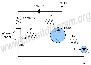
This is a remote tester circuit designed to test TV and other remote controls. The circuit is simple and utilizes only a few components. The infrared sensor used in the circuit is the TSOP1738. When the infrared waves are...

The 555 timer is a highly versatile integrated circuit that has found applications in a wide range of devices, from toys to spacecraft. This chip can function as an oscillator, a Schmitt trigger, and more. The 555 timer is a...

Many antique radios operate on batteries, including tube portables like the Zenith model K-401 and "farm" radios used in rural areas without electrical power. This article provides historical context on battery usage in early radios and offers guidance on...
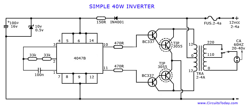
An article on how to create an inverter using a simple 40-watt inverter circuit diagram and schematics. This inverter converts 12 volts to 220 volts using the CD4047 integrated circuit. The described inverter circuit utilizes the CD4047 IC, which is...
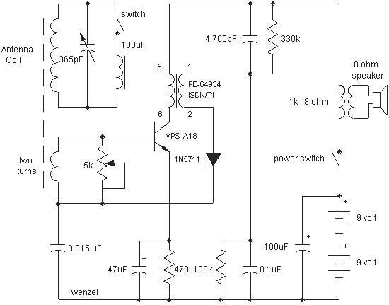
This reflex radio project was inspired by Robert Bazian's design. His reflex radio is the "darndest" thing I have seen and his spectacular results inspired me to come up with my own version! These designs are similar to two-transistor...

This application note presents the component values and measured performance for the MAX2681 mixer IC when tuned for GPS operation at 1575 MHz. The MAX2681 is a high-performance mixer integrated circuit designed for use in GPS applications, particularly at the...