
FET BALANCED MODULATOR FOR SSB

The described circuit employs matched FETs in a push-pull configuration, which is advantageous for achieving high efficiency and low distortion in modulation applications. The use of transformer T1 with a center-tapped secondary winding allows for effective coupling of the AF modulating signal to the gates of the FETs, ensuring that both devices operate in a complementary manner. The parallel connection of the RF carrier to the sources through capacitor C3 permits the RF signal to be present while isolating the audio frequency components.
The cancellation of the RF carrier in the output circuit is a critical aspect of this design, as it ensures that only the modulated sidebands remain, which carry the information from the AF signal. This is achieved through careful design of the output stage, which may include filters or other components to remove the carrier frequency while preserving the integrity of the sidebands.
Resistor R3 plays a pivotal role in maintaining balance within the circuit. Variations in component values or characteristics can lead to imbalances that affect performance, particularly in push-pull configurations where symmetry is essential for optimal operation. By adjusting R3, the designer can compensate for these discrepancies, ensuring that both FETs operate effectively and that the output signal remains clean and distortion-free.
This circuit is particularly relevant in applications such as amplitude modulation (AM) transmitters, where the quality of the modulation directly impacts the performance of the transmission. The careful selection and configuration of components, along with the implementation of balancing techniques, contribute to the overall effectiveness and efficiency of the modulation process.AF modulating signal is applied to gates of matched FETs in push-pull through T1 having accurately center-tapped secondary, and RF carrier is applied to sources in parallel through C3. Carrier is canceled in output circuit, leaving two sidebands. R3 is adjusted to correct for un-balance in circuit components. -R. P. Turner, "FET Circuits, " Howard W . Sams, Indianapolis, IN, 1977, 2nd Ed. , p 90-91. 🔗 External reference
Related Circuits

This circuit utilizes a MOSFET amplifier as the primary component for boosting audio signals. It is designed to drive a speaker with an impedance of 8 Ohms and a power output exceeding 200W. Additionally, a suitable power supply circuit...
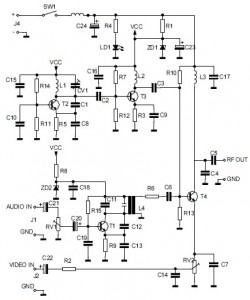
This is the circuit diagram of an audio/video modulator. The circuit converts audio and video signals into a UHF TV signal, allowing a video signal from a camera or other source to be connected to a standard TV set....
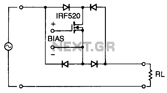
Utilizing four diodes in an array enables the use of a single MOSPOWER transistor for analog switching. The current flow is managed by maintaining the source-base connection of the MOSFET towards the load. It is essential to select diodes...
This FET voltmeter (FETVM) serves as a replacement for the vacuum tube voltmeter (VTVM) and eliminates the need for a standard line cord. Additionally, the drift rates of field-effect transistors (FETs) are significantly better than those of vacuum tube...
This circuit is a series-FET Voltmeter known as FETVM. The FETVM is designed to replace the function of a vacuum tube voltmeter (VTVM) while simultaneously providing a means to clean the appliance cord. Additionally, the drift rate of this...
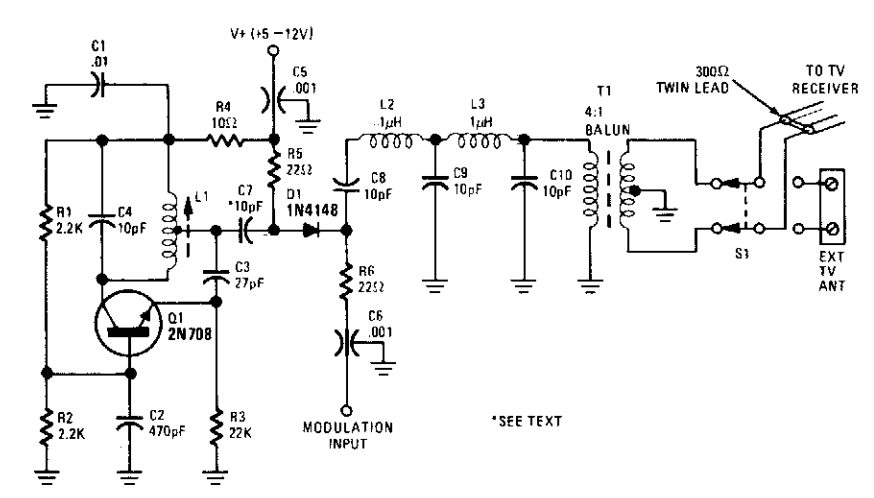
This circuit allows for the direct connection of composite video signals from video game consoles and microcomputers to the antenna terminals of television sets. The output signal level is regulated by the modulation input. The circuit design effectively integrates composite...