
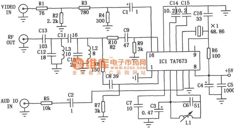
Video modulator 2

The circuit design effectively integrates composite video signals into the existing infrastructure of television sets by utilizing the antenna input. This is particularly beneficial for older television models that may not have dedicated composite video inputs. The primary components of the circuit include a modulation input, which adjusts the output signal level, ensuring compatibility with various television models and optimizing signal clarity.
The composite video signal is typically a combination of video information encoded in a single channel, which includes luminance (brightness) and chrominance (color) data. The circuit may incorporate a buffer amplifier to ensure that the signal maintains integrity over longer distances and to prevent signal degradation. Additionally, passive components such as resistors and capacitors may be employed to filter the signal, reducing noise and enhancing overall video quality.
The modulation input can be implemented using a variable resistor or a potentiometer, allowing users to fine-tune the output level according to their specific requirements. This feature is crucial, as different television sets may respond differently to the incoming signal strength.
Overall, the circuit serves as a practical solution for connecting modern video sources to legacy television equipment, facilitating the enjoyment of video games and computer displays on older screens while maintaining optimal signal quality.This circuit permits direct connection of composite video signals from video games and microcomputers to the antenna terminals of TV sets. The output signal level is controlled by the modulation input. 🔗 External reference
Related Circuits

This circuit is a Phase-Locked Loop (PLL) system designed to function as an FM demodulator. The output of the Voltage-Controlled Oscillator (VCO) tracks the FM signal, and since the input voltage of the VCO is proportional to its output...

A gate voltage is applied to initiate the process. When the gate voltage is in the ON state, Q1 is activated, and capacitor C is charged through the attack potentiometer in series with the 1 kΩ resistor. By adjusting...
The RF modulator is a crucial component in televisions, VCRs, satellite receivers, format converters, home computers, and gaming consoles. This circuit is straightforward, stable, and easy to construct, allowing for seamless integration with various circuit boards. The schematic diagram...
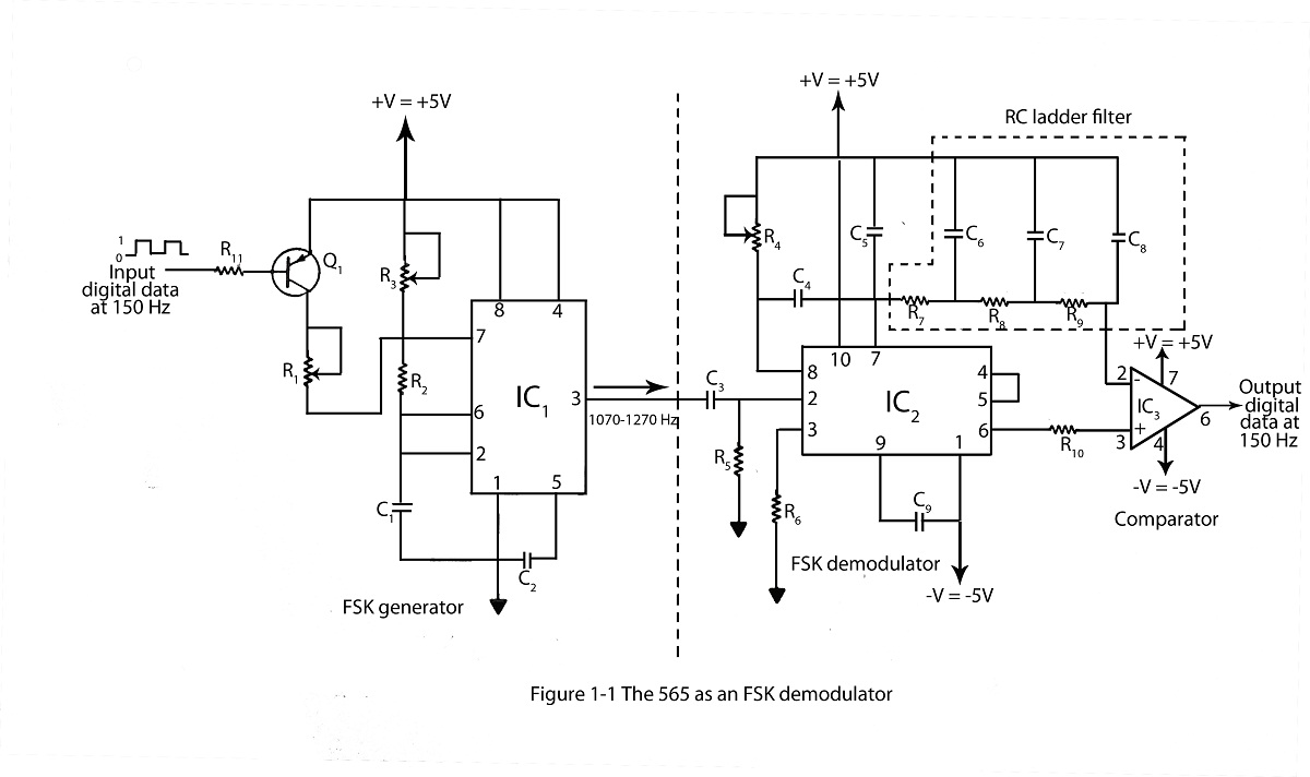
The frequency shifting keying technique is utilized to transmit binary data. The circuit diagram includes a description of an FSK demodulator that employs the 565 integrated circuit for frequency shift keying. The frequency shift keying (FSK) technique is a form...
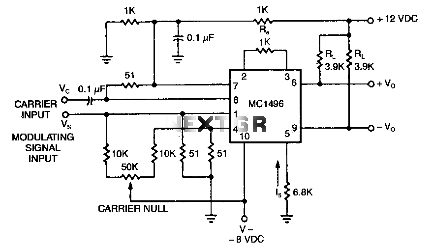
The basic current allows no carrier to be present in the output. By adding offsets to the carrier differential pairs, controlled amounts of carrier appear at the output. The amplitude becomes a function of the modulation signal - AM...
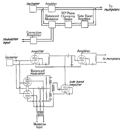
A system is being developed to transmit in the FM band. The oscillators have already been constructed to facilitate transmission across multiple frequencies. The design of an FM transmission system involves several key components, including oscillators, modulators, amplifiers, and antennas....