
clic 555 timer chip schematic

The 555 timer IC is a versatile and widely used component in electronic circuits, known for its ability to function in various modes such as astable, monostable, and bistable configurations. The classic schematic representation of a 555 timer circuit typically includes the IC itself, along with essential passive components like resistors, capacitors, and sometimes diodes, depending on the intended application.
In the astable mode, the 555 timer operates as an oscillator, generating a continuous square wave output. This configuration involves connecting two resistors (R1 and R2) and a capacitor (C1) to the appropriate pins of the IC. The output frequency can be calculated using the formula:
\[
f = \frac{1.44}{(R1 + 2R2) \cdot C1}
\]
In monostable mode, the 555 timer is triggered by a short pulse on the trigger pin, producing a single output pulse of a defined duration. The time period of this pulse is determined by the resistor (R) and capacitor (C) connected to the discharge and threshold pins, calculated using:
\[
T = 1.1 \cdot R \cdot C
\]
In bistable mode, the 555 timer acts as a flip-flop, providing two stable states. This configuration typically requires two trigger inputs and can be used in applications such as toggling switches or memory storage.
The schematic for the 555 timer circuit includes clear labeling of power supply connections, ground, and output, ensuring ease of understanding and implementation. The design is often accompanied by annotations indicating the values of resistors and capacitors, as well as the expected output behavior under various conditions. This makes it an excellent educational tool for both novice and experienced electronics enthusiasts, highlighting the functionality and versatility of the 555 timer IC in practical applications.classic 555 timer chip schematic circuit t shirt by eevblog picture on VisualizeUs - Bookmark pictures and videos that inspire you. Social bookmarking of pictures and videos. Find your pictures and videos.. 🔗 External reference
Related Circuits

The PWM Output section has been separated into the upper left corner, delineated by a heavy purple line that is bridged by jumper JP1 on the APM2.0. This design choice highlights that diode D1 allows current to pass through...
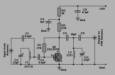
This is a simple circuit of an FM booster designed to enhance the reception of programs from distant FM stations. The amplifier effectively captures signals from far-off FM stations. The configuration is set up as a common-emitter tuned RF...
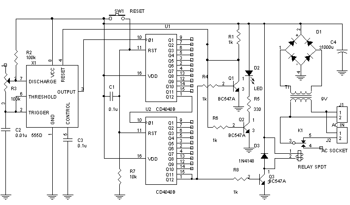
The following schematic diagram is a four-hour timer circuit. Features include ease of construction, a total timing duration of 3 hours and 53 minutes, and a 9V supply voltage. Components utilized in the circuit are a 555 timer IC,...
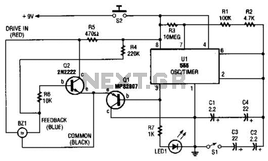
The electronic darkroom timer is constructed using a 555 oscillator/timer, a pair of general-purpose transistors, a buzzer, and an LED. The 555 timer (U1) is set up as an astable multivibrator, functioning as a free-running oscillator. The frequency of...

The following page outlines detailed information and the schematic of the 1985 Pontiac Fiero Wiring Diagram and Electrical System. The electrical system consists of: The 1985 Pontiac Fiero features a complex electrical system designed to support various components and functionalities...

This voltage-to-frequency converter (VFC) circuit utilizes a 555 integrated circuit (IC) and a 741 operational amplifier (op-amp) as its primary components. The circuit is capable of generating oscillations of up to 20 kHz. The voltage-to-frequency converter circuit is designed to...