
clk3 binary alarm clock

The electronic circuit described functions as a basic digital clock with alarm capabilities. The LM7805 voltage regulator is a crucial component, converting a higher input voltage (ranging from 7V to 35V) to a stable 5V output, which is essential for powering the MCU and other components. The design utilizes a microcontroller programmed in assembly language, allowing for efficient control of the clock's operations.
The ICSP feature enables easy reprogramming of the MCU, facilitating updates or modifications to the clock's firmware. The switch S5 serves as a mode selector, allowing the user to toggle between programming and clock operation modes. The inclusion of multiple buttons (S1 to S4) provides intuitive user interaction for setting time and alarms, enhancing the overall usability of the device.
The use of PORTA, PORTC, and PORTD for driving the LEDs indicates a well-structured approach to managing the output display. Each port is utilized for specific time intervals (hours, minutes, and seconds), ensuring that the circuit can visually represent the current time effectively.
The design consideration regarding the diode D21 is noteworthy, as it highlights the importance of understanding current flow in the circuit. The separation of GND and Vss during programming ensures that the programming process does not interfere with the normal operation of the clock, maintaining the integrity of both functions.
Overall, this circuit exemplifies a blend of foundational electronic principles with practical application, showcasing the capabilities of microcontrollers in building functional and interactive devices.This is the first electronic circuit I designed from scratch, my first time programming a MCU, the first time I wrote an application in assembly language and my second homemade PCB. Usually people starts building very simple things and they increase the complexity of their work a bit at a time, but I prefer to learn and build things much more comp
lex than I am (theoreticaly) capable of, so I learn and work much more faster. Input 7-35V is converted to 5V using a LM7805. The MCU can be programmed by ICSP plugging the programming cable to P2 and activating positions 6 and 7 of S5 and deactivating the rest of them. For using the circuit in clock-mode (not programming-mode) positions 1-5 of S5 must be activated and 6-7 deactivated.
LEDs used to show the hours are connected to PORTA, those used to show minutes to PORTC and for seconds to PORTD. Button S1 rises the time one hour, S2 one minute, S3 sets up the actual time and S4 the alarm time. The diode D21 seems to be upside down but it isn`t because P1 is the power jack, so current must flow from the GND of the circuit to P1-1 which is the ground of the external power.
The circuit has two ground lines: GND and Vss. Usually (clock-mode) they are shorted but they are split when the PIC is being programmed so Vss (ground of the ICSP programmer) is completely isolated from the rest of the circuit. 🔗 External reference
Related Circuits
This burglar alarm system circuit utilizes an infrared proximity detector that triggers an alarm when the rays falling on its sensor are interrupted. It stands out from other burglar alarm systems due to its simplicity as a DIY project,...
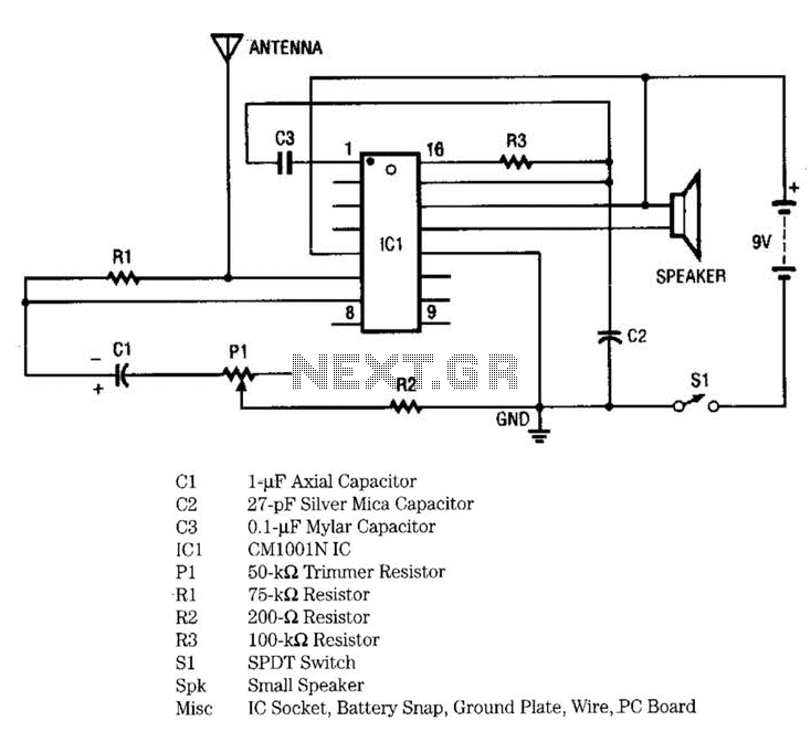
IC1 includes multiple oscillators and an amplifier. The low-frequency audio signal oscillator provides an input to the amplifier. This signal is the audio tone that is amplified and subsequently delivered to the speaker by the amplifier. The high-frequency oscillator...
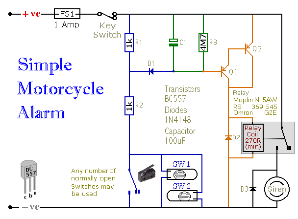
When one of the switches is closed, the base of Q1 is connected to ground through D1 and R2. This activates Q1, which in turn activates Q2. Q2 connects the positive side of the relay coil to the supply...
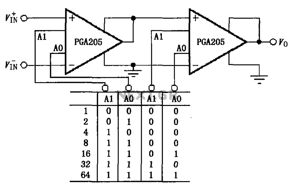
A binary gain step circuit is illustrated using the PGA205, which has a gain range of 1 to 64. The circuit employs two PGA205 devices in cascade, resulting in a total gain that is the product of the individual...

A filtered 15 V DC supply is applied to a series circuit that includes a thermistor (R2) and a parallel combination of resistors (R1 and R3). The transistor (Q1) functions as a switch, with its state controlled by the...

Transistors are configured as a Darlington pair in this circuit. A thermistor is utilized to detect or sense heat. A 12K variable resistor is employed to adjust the activation of the buzzer at the desired temperature. The operation of...