
Cmos Piezo Driver Using 4049 Circuit

The circuit design begins with the 4049 IC, which is a hex inverter capable of converting input signals into corresponding output signals. Each inverter within the IC can be utilized to control the base of the 2N2222 transistor. The 2N2222 is a versatile NPN transistor commonly used for switching applications due to its ability to handle moderate currents and voltages.
The piezo transducer, referred to as crystal 1 in this context, is an electromechanical device that converts electrical energy into mechanical vibrations, generating sound waves. When the transistor is activated by the output from the 4049 IC, it allows current to flow from the collector to the emitter, effectively powering the piezo transducer.
In this circuit, proper biasing of the 2N2222 transistor is crucial to ensure it operates in the saturation region when activated. This involves connecting a resistor in series with the base of the transistor to limit the base current while ensuring sufficient current to switch the transistor fully on. The output from the 4049 IC should be designed to provide a suitable voltage level to turn on the transistor, typically around 0.7V for silicon transistors like the 2N2222.
The overall functionality of this circuit can be enhanced by adding additional components such as capacitors for noise filtering, diodes for flyback protection (if inductive loads are involved), and resistors to set the gain and operating conditions of the transistor. This configuration allows for efficient control of the piezo transducer, enabling various applications such as sound generation in alarms, notifications, or signal transmission in electronic devices. This circuit uses a 4049 IC to drive a 2N2222 switching transistor. The transistor drives crystal 1 a piezo transducer.
Related Circuits

When utilizing a regulated power supply to decrease voltage, there exists a risk of component failure within the supply, potentially resulting in damage to connected equipment. While a fuse can provide protection against excessive current draw, it may not...
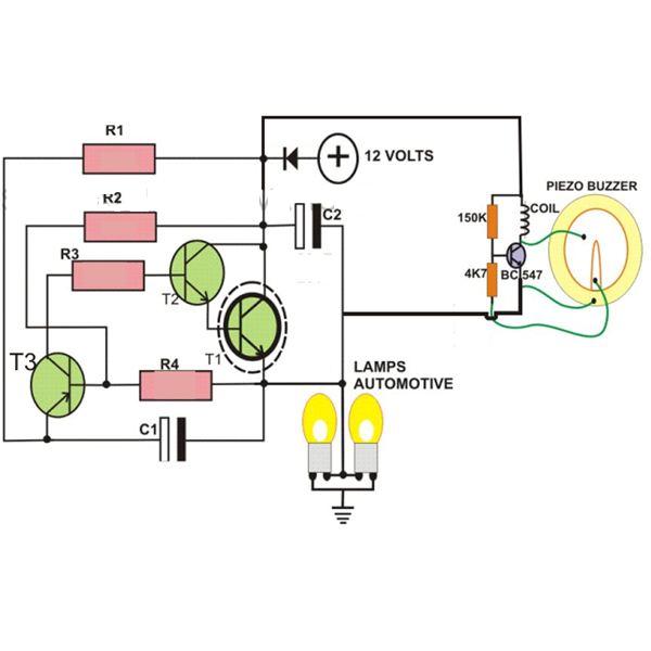
This circuit is designed to create a flasher unit for a motorbike. It is a simple turn signal flasher circuit that can be easily built and installed in any two-wheeler for the desired functionality. The circuit uses only two...

Figure 3-16 illustrates a low-noise preamplifier equalizing circuit using the HA12017. This circuit includes playback components R3, R4, and C4, which conform to a standard balanced network. The gain of the circuit is -7dB at 1kHz, while the output...

The performance indices of the telecontrol receiving decoding circuit are as follows: radio frequency (f) = 27 MHz, audio frequency (f) = 5.5 kHz, 100% modulation in square-wave form; radio frequency deviation is ±600 Hz, and the frequency shift...

The diagram illustrates a series connection of cell diode capacitors, each rated for an increasing voltage of 300 V. This configuration generates a high DC voltage supply of 40 kV, which can be utilized for various experimental applications. With...

The basic connection circuit for the INA166 includes signal and power connections. A 0.1 µF tantalum capacitor should be used for filtering the chip's power supply terminal, and the PCB layout should be designed to position this capacitor as...