
CS63 Programming Project

The 8x8-bit memory module is a crucial component in digital systems, designed to efficiently store and retrieve data. The choice of using 688 logic gates indicates a careful balance between complexity and functionality, allowing for effective data handling without overwhelming the design. The use of abstraction layers simplifies the representation of the circuit, making it easier for users to understand the operation of the memory module.
The input switches (L0-L7) provide a means for users to enter 8-bit data into the memory. The address switches (A0-A2) allow for the selection of one of the eight memory locations for read or write operations. The chip enable (CE) signal activates the memory module, while the read/write (RW) signal determines whether data is being written to or read from the memory. The output enable (OE) signal is essential for controlling when the data output is valid.
The 3-to-8 decoder plays a pivotal role in the design, translating the 3-bit address input into a corresponding output that activates one of the four memory modules at a time. Each memory module is capable of storing four 8-bit words, effectively allowing the entire memory module to manage a total of eight 8-bit words.
The final output from the memory modules is processed through an OR gate, which combines the outputs of the selected memory modules, ensuring that the correct data is sent to the CPU. This design choice is crucial for maintaining data integrity and ensuring that the CPU receives the desired information.
Simulation results on the PowerMac 7100/80 demonstrate the functionality of the design, confirming that the module operates as intended. The inclusion of custom module diagrams further aids in understanding the internal workings of the memory system, providing a comprehensive overview of the design's architecture and operation. The overall design reflects a well-thought-out approach to memory module architecture, balancing complexity and usability for effective data management in electronic systems.I designed a 8x8-bit memory module using LogicSim, a shareware software program that allows people to create logic diagrams and run a simulation using that design. The memory module I created uses 688 logic gates. There are couple layers of abstraction in the design. I did this for two reasons. First, I wanted to keep the diagram as well organized and as understandable as possible. The other reason was LogicSim does not have a big desktop. Abstraction allowed me to put more words into the memory module. Initially I tried implementing a 7x8-bit memory module (see below). However, that used 938 logic gates. It was a monster. Then I tried at 12x8-bit module. When I tried to run a simulation using the circuit, it crashed the program, so I abandoned that idea. So I settled on the 8x8-bit memory module. This diagram of this module is simpler and easier to follow, compared to my original 7x8-bit module. By the way, the goliath fell hard. This memory module contains 688 logic gates, a far cry from 938. The goliath also suffered from a major flaw. A word in memory was purged when either the RW or CE inputs were changed. I believe I fixed that bug. Please look at my design for a 8x8-bit memory module and tell me what you think. I included the circuit diagrams for the custom modules used in the main circuit diagram. Let me try to explain this diagram so it is less confusing. On the left are many switches. The switches labeled L0-L7 are data input switches. The switches labeled A0-A2 are address switches. CE, RW, and OE stand for chip enable, read/write, and output enable, respectively. The address lines feed into a 3-8 decoder, which determine which word is to be enabled for reading or writing.
The output from the decoder feeds into the 4x4-bit memory modules, which are custom-made. The data lines, as well as CE, RW, and OE, also feed into the memory modules. The modules are labled W0-W3 and W4-W7. That means the module W0-W3 are used to store words 0 through 3 and likewise with W4-W8. Two modules are used to store 4 8-bit words. The output from the memory modules are the values for bits 0 to 7. I should note that although the memory modules have their inputs marked as 0 through 3 and their outputs marked as 0 through 3, only one pair of modules actually stores the values for bits 0 through 3. The other pair stores the values for the bits 4 through 8. The output from the memory modules, are paired and the pair is run through an OR gate. The result is the value memory would send to the CPU. I hope that clears up some things. I tried running a simualtion of the circuit on a PowerMac 7100/80. The circuit diagram you see above is a snapshot of a simulation of the circuit. I have also include circuit diagrams of the custom made modules which are also snapshots of simulations.
Enjoy! 🔗 External reference
Related Circuits

The hobby circuit described utilizes a unique approach to generate approximately 12,000 volts with a current of about 5 µA. It employs two silicon-controlled rectifiers (SCRs) that form dual pulse generator circuits. These SCRs discharge a 0.047 µF capacitor...
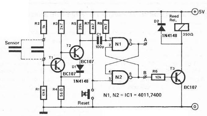
This humidity detector circuit diagram is straightforward and utilizes a limited number of components. It can be employed to activate electronic devices when the detector identifies a specific humidity level. The sensor is made from two copper pieces positioned...
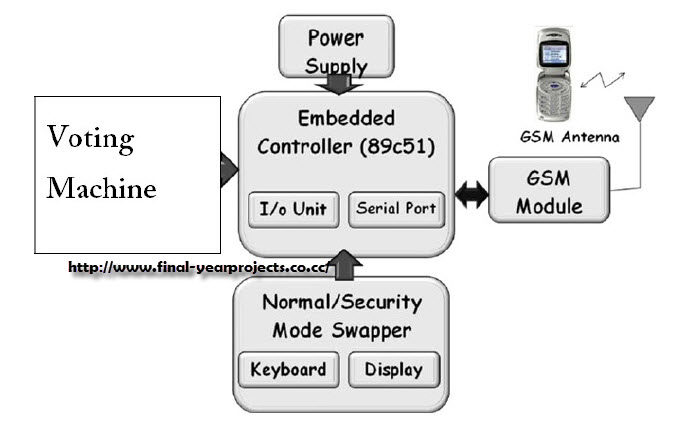
This project involves a GSM-based voting machine system that utilizes AT commands to send SMS through a microcontroller. It operates in two modes: Normal mode, where an authorized individual from a local area can cast their vote, and Security...

The LM35 Smart Heater Controller Schematic features a compact circuit designed around the well-known 3-Pin Integrated Temperature Sensor LM35 (IC1) from National Semiconductor. Additionally, a widely used BiMOS Op-amp CA3140 (IC2) is employed to monitor the temperature sensor's output,...
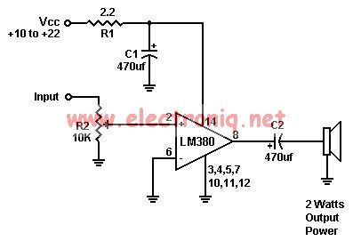
A simple audio amplifier can be designed using the LM380 along with a few external components. This amplifier features a wide supply voltage range, an input impedance of 150 kΩ, low distortion, and a current capability of 1.3 A. The...
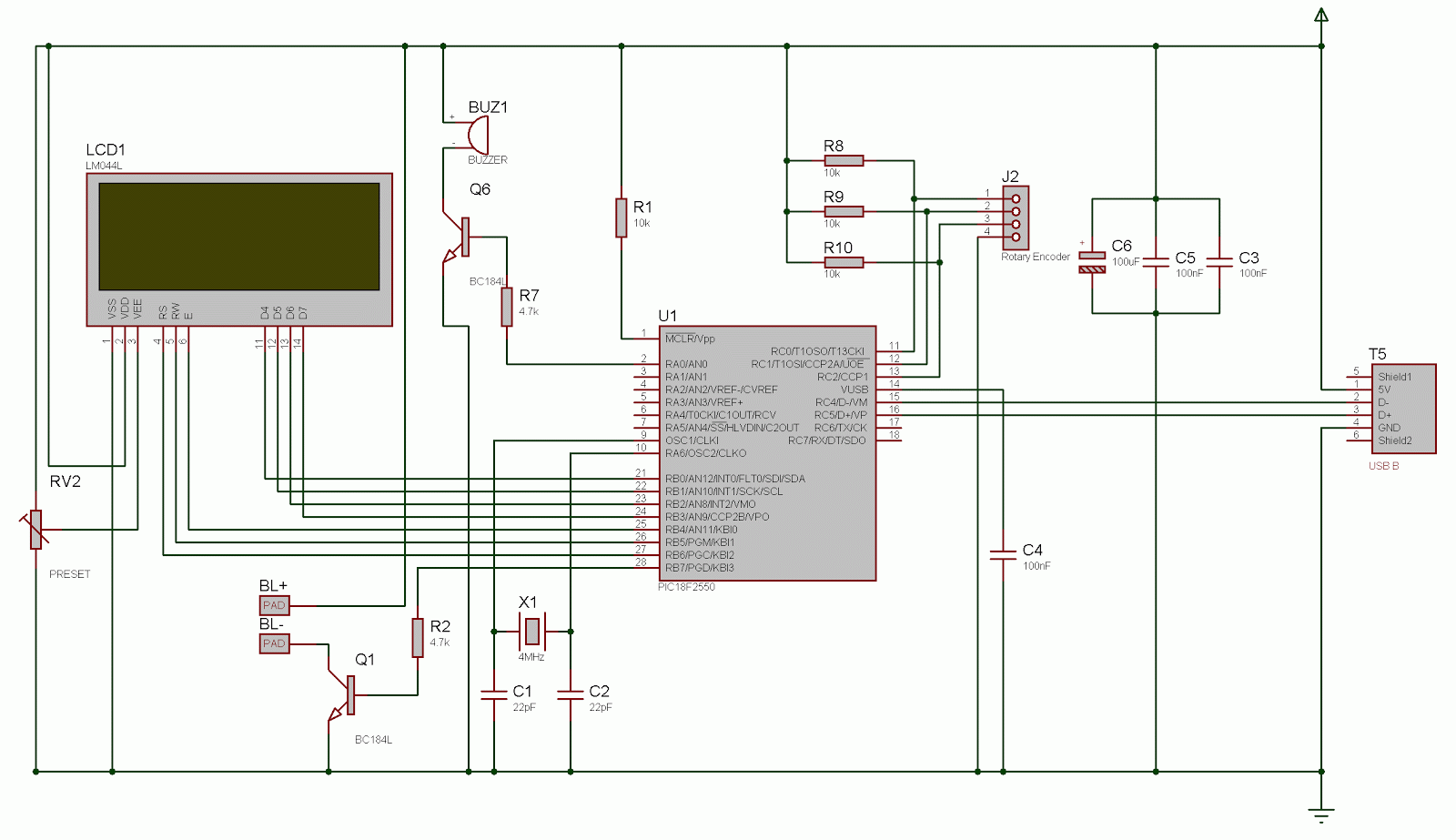
This project involves a USB interface for an alphanumeric LCD display, such as the 4x20 model, which can be controlled using the LCD Smartie program. The USB interface is implemented with the PIC18F2550 microcontroller and utilizes USB LCD modules....