
Data Transfer interface

On the DS interface side, the firmware provides for weak internal pull-ups on the Attention and Data lines, so no external resistors are required unless there is a large capacitive load on these lines, in which case resistors as low as 270 Ohms may be used.
The DS protocol enables effective communication between a host microcontroller and slave devices in scenarios where dedicated hardware interfaces are not available. The two I/O ports required for this protocol can be configured flexibly, allowing for various implementation strategies depending on the available resources of the microcontroller. The firmware-driven nature of this protocol facilitates adaptability in terms of communication timing and data handling, enabling operations even in low-power or resource-constrained environments.
In practical applications, the 5V power pin serves a dual purpose: it not only powers the DS device under test but also simplifies the circuit design by reducing the need for additional power supply components. Implementing a power switch enhances usability by allowing power control during testing or development phases.
The requirement for precise timing is emphasized in the context of the AT902313's baud rate generator, highlighting the importance of synchronization in serial communications. The use of RS-232 inverters, such as the Maxim MAX-232, is a common practice in interfacing with standard serial communication protocols. These inverters are compact and allow for efficient signal level conversions, making them suitable for hand-built circuits.
The firmware's provision of weak internal pull-ups on the Attention and Data lines is a significant feature that reduces the component count in the design. However, in scenarios where external capacitance may affect signal integrity, the inclusion of external resistors becomes necessary to maintain reliable communication. The suggested value of 270 Ohms serves as a guideline to mitigate potential issues arising from capacitive loading, ensuring that the signals remain within acceptable voltage levels for proper device operation. This design consideration is crucial for maintaining the robustness of the DS communication protocol in diverse applications.The DS protocol was designed to provide firmware-based bidirectional host-to-slave inter processor communications for situations in which no hardware solution is available and the host and/or the slave in incapable of tending the interface in real time. The only specialized hardware required is two bidirectional I/O ports on each chip (alternatively two input ports and two tri-statable output ports may be used.
In other words, it provides some of the functionalit of the Two-Wire-Interface (TWI, or I2C as named by Philips) where an actual TWI is not feasible in either hardware or firmware. The 5 volt power pin on the DS interface may be used to supply power to the DS device being tested. In this case, a power on-off switch would be a good idea. The microcontroller timing is unimportant for the DS device, but it is critical for the baud rate generator on the AT902313. The RS-232 inverters could also be Maxim MAX-232 or something similar. I prefer these discreet inverters because I am building them by hand and they take less board space than the DIP buffers.
On the DS interface side, the firmware provides for week internal pullups on the Attention and Data lines, so no nexternal resistors are required unless there is a large capactive load on these lines, in which casce, resistors as low as 270 Ohms may be used. 🔗 External reference
Related Circuits
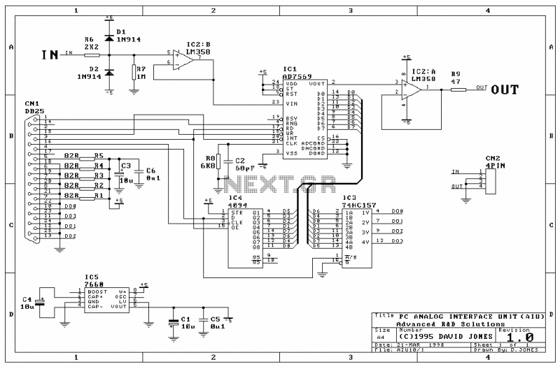
The Analog Interface Unit (AIU) is a simple circuit that connects to a PC parallel port, and allows you to sample and output 8-bit analog signals under software control. More: Here are some of the features: 8-bit ADC and...
The CAN Bus interface utilizes an asynchronous transmission scheme that is regulated by start and stop bits at the beginning and end of each character. This interface operates using serial binary interchange, allowing information to be transmitted from transmitters...
An electrocardiogram (ECG), also known as EKG (derived from the German term Elektro-Kardiographie), is an electrical recording of the heart utilized in diagnosing heart disease. This application employs a DrDAQ Data Logger to read and store electrocardiograms. British physiologist...
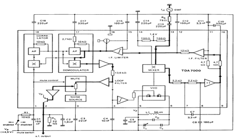
The TDA7000 is an integrated circuit (IC) designed for FM portable radios, featuring a Frequency-Locked Loop (FLL) system with an intermediate frequency of 70 kHz. It incorporates several functions, including an RF input stage, mixer, local oscillator, IF demodulator,...

This system is designed to communicate or transmit a text message from one location to another using a wireless circuit. The text message is encrypted with a microcontroller, and the encrypted message is transmitted wirelessly. At the receiving end,...
A clock-and-data recovery (CDR) circuit is utilized to recover the clock from a transmitted data stream and re-time that data with the recovered clock. These circuits are generally positioned at the front-end of receiver chips to extract the clock...