
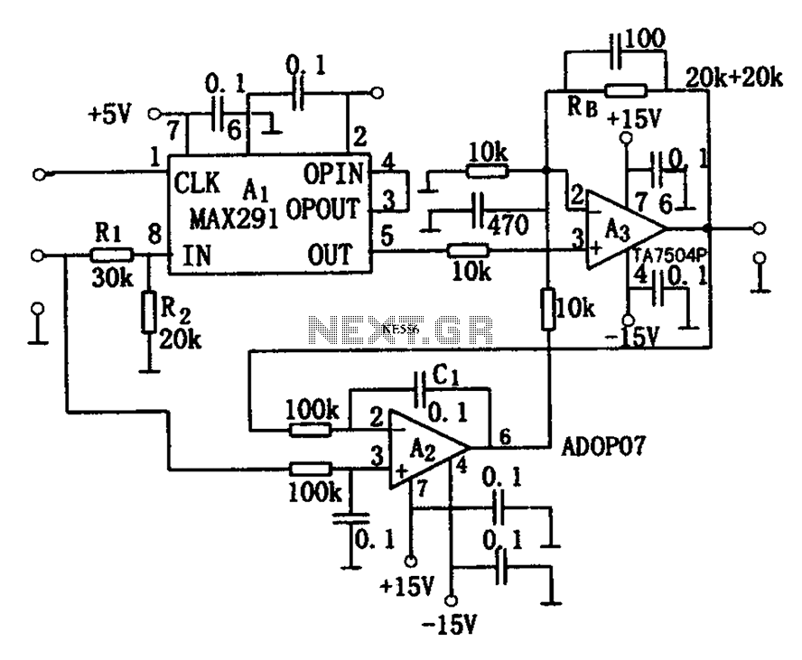
DC accurate low-pass filter

The LTC1050 is a precision operational amplifier designed for low noise and low offset applications, configured here as a second-order low-pass filter. The filter is set to unity gain, which means that the output voltage will follow the input voltage without amplification. The center frequency of the filter is calculated using the formula (1.2πR´C´), which results in a cutoff frequency of 17.2 Hz, with a quality factor (Q) of 0.5. This design choice ensures a smooth transition of frequencies, characteristic of Bessel filters, which are known for their minimal phase distortion and well-behaved transient response.
The power supply voltage is specified as ±8V, which allows for a common-mode input range of ±6V. This is critical for maintaining linearity and avoiding distortion in the output signal. The low noise performance of the LTC1050 is highlighted by a measured wideband noise of 52μVrms, making it suitable for applications where signal integrity is paramount.
For applications requiring a higher order filter, the design can be modified easily by adjusting the clock frequency and the resistor and capacitor values. For example, a 7th order Butterworth filter can be implemented with a clock frequency (fCLK) of 1 kHz, and specific values for resistors (R = 26.7k, R´ = 165k) and capacitors (C = 1μF, C1 = 0.2μF, C2 = 0.047μF).
The LTC1062, mentioned in the context, serves as a complementary device that employs an external resistor-capacitor network to isolate the integrated circuit from the DC path of the input signal. This configuration is particularly advantageous as it mitigates DC offset issues commonly associated with monolithic switched-capacitor filters, enhancing the overall performance for DC accurate applications.
In addition, the LTC1062's architecture allows for antialiasing of incoming signals, ensuring that signals larger than half the clock frequency do not adversely affect the filter's performance. The integration of high-performance chopper-stabilized operational amplifiers with the LTC1062 further enhances its utility in precision applications.
Finally, the design incorporates a diode at pin 3 of the LTC1062 to protect against incoming signals that exceed the power supply levels, safeguarding the integrity of the circuit. The internal capacitors of the LTC1050 not only reduce the footprint on the PCB but also help in minimizing the residual clock noise, maintaining the overall signal fidelity without introducing additional DC errors.The LTC1050 is confi gured as unity gain 2nd order low-pass fi lter which center frequency is (1.2πR´C´) = 1.72 • fCUT-OFF = 17.2Hz and Q = 0.5. Figure 2 shows the amplitude response of the fi lter, and Figure 3 shows a well behaved transient response for which Bessel fi lters are famous.
The power supplies used were ±8V to provide a total DC input common-mode range of ±6V. The measured wideband noise was 52μVrms. The clock, and R, C values of Figure 1 can be easily modifi ed to provide a 7th order Butterworth 10Hz fi lter, such as: fCLK = 1kHz, R = 26.7k, C = 1μF, R´ = 165k, C1 = 0.2μF and C2 = 0.047μF. The diode at LTC1062 pin 3 should be used to protect the device from incoming signals above the power supplies.
Monolithic switched-capacitor low-pass fi lters, although they offer precise frequency responses, cannot usually be used for DC accurate applications because of their prohibitive DC offsets and poor gain linearity. The LTC®1062, however, is quite different from currently available low-pass switched capacitor fi lters because it uses an external (R, C) to isolate the IC from the input-signal DC path and to provide antialiasing for incoming signals larger than half its clock frequency.
The LTC1062 is ideal when used in conjunction with high performance chopper-stabilized op amps. The LTC1050 is an ultra low offset, low noise chopper with the sampling capacitors internal. It can remove residual clock noise without adding further DC error. Also, the internal capacitor minimizes board area. 🔗 External reference
Related Circuits
To create a Butterworth low-pass filter with a 12 dB/octave roll-off, four second-order (12 dB/oct) filter blocks are connected in series. This configuration is intended to achieve flat response characteristics across the frequency spectrum. The values for each stage...
Seeking the appropriate resistor and capacitor values for a low-pass filter designed to eliminate radio frequency (RF) interference. The application focuses on filtering out unwanted untuned RF signals from a crystal radio set. A low-pass filter is an essential component...

The circuit diagram illustrates a simple subwoofer filter designed to operate with a 12V DC supply, making it particularly useful for automobile subwoofer applications. This circuit functions as a low pass filter, with an adjustable pass frequency ranging from...
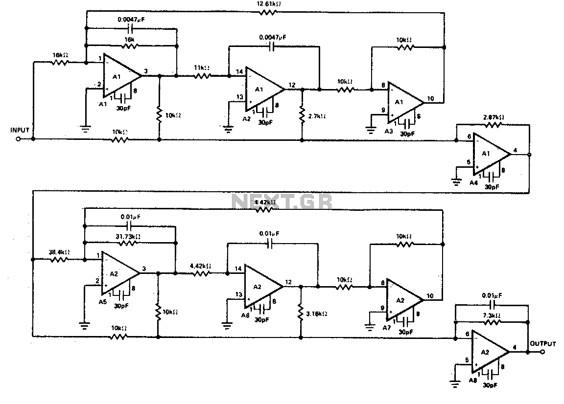
The realization of a type 03 receive filter is achieved using eight OP-08 operational amplifiers. The response curve indicates that the requirement for greater than 30 dB attenuation in the stop band has been satisfied. Furthermore, the noise performance...
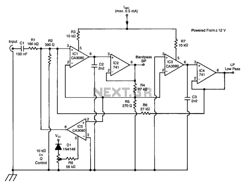
A standard dual integrator filter can be constructed using a few CA3080 operational amplifiers. By varying the parameters L, A, B, and C, the resonant frequency can be swept over a range of 1000:1. At IC1, three current-controlled integrators...
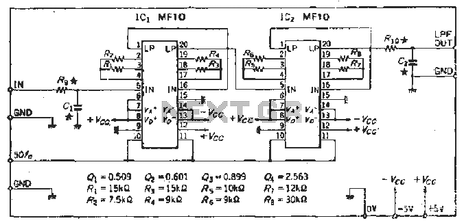
The circuit depicted in Figure 8 is a low-pass filter utilizing an eight-stage switched-capacitor configuration. The cutoff frequency of the circuit can be adjusted, with a clock frequency that can be modified to 1/100 of the original frequency. A...