
Delay circuit diagram of energy-saving lamps

The delay-saving lamp circuit is designed to enhance energy efficiency and convenience in lighting applications. The core functionality involves the integration of sound detection to control the lighting based on ambient conditions. The circuit operates by utilizing a diode bridge rectifier (VD1 to VD4) that converts the AC supply voltage into a pulsating DC voltage. The subsequent regulation by the zener diode (VD5) ensures a stable 8V output, which is essential for powering the NAND gate (CD4011) and the transistor (VT7).
The NAND gates, configured in a suitable logic arrangement, process the input signals from the microphone and the photosensitive resistor. The microphone (B) picks up sound signals, which are amplified and processed to trigger the lighting system. The photosensitive resistor (GR) detects ambient light levels, preventing the lights from activating during the day or in bright environments.
The adjustable timing circuit, facilitated by the capacitor (C3) and associated resistors, allows for a customizable delay before the light turns off, catering to various user preferences. The resistors (R1 to R7) are strategically chosen to set the appropriate thresholds for sound detection and timing. The use of potentiometers (RP) enables fine-tuning of the sensitivity and delay settings.
In terms of component selection, the circuit uses reliable and readily available electronic components. The silicon diodes (1N4007 and 1N4148) are chosen for their robustness and efficiency in rectification and switching applications. The thyristor (MCR100-8) is selected for its capability to handle the load and provide control over the light output. The NPN transistor (9013) is utilized for its amplification properties, ensuring effective control of the load based on the logic outputs from the NAND gates.
Overall, this delay-saving lamp circuit is an effective solution for energy-efficient lighting control, providing automated lighting in response to sound and light conditions, thus enhancing safety and convenience in various environments.Delay saving lamps as shown is a sound and light control delay energy-saving lighting double. It can directly replace ordinary light switch without changing the original lighti ng circuits, day or strong light situations even greater sound can also control the bulb does not light, sound encountered at night or low light (such as voices, footsteps sound, etc.) after the lights turn on automatically, after about 30s (time can be set) automatically turn off. Suitable for staircases, corridors and other places lighting just short. Diode VD1 ~ VD4 bridge rectifier circuit composed of the city into a pulsating DC power, and then by limiting R7, VD5 regulator, C3 filtered output 8V DC, for the manifold CD4011 and provide power transistor VT7.
Component selection: NAND gate D1 ~ D4 is available a 2-input NAND gate CD4011 four digital integrated circuits. VS is MCR100-8 type and other small plastic unidirectional thyristors. Rectifier diode VD1 - VD4 available 1N4007 type silicon rectifier diode ordinary, VD5 election 2CW56 type 8V zener diode, VD6 common type available 1N4148 silicon switching diodes, VT7 available 9013 type and other silicon NPN transistor.
GR is MG45 photosensitive resistor, the remaining resistors are used RTX-1/8W carbon film resistors, wherein R1 is 22k, R2 is 22M, R3 is 33k, R4 is 47k, R5 is 1.5M, R6 is 5.10, R7 is 240k, RP take W106-2-2 type 100k glass glaze preset potentiometers. C1 with CT1 type ceramic capacitors, C2, C3 electrolytic capacitors C1 and take 0.1 F, C2 take 22 F/16V, C3 take 100 F/16V.
B is CRZ2-113F type electret condenser microphone.
Related Circuits
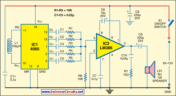
This multi-tone siren is beneficial for burglar alarms, reverse horns, and similar applications. It generates five distinct audio tones, making it more attention-grabbing than a single-tone siren. The circuit is designed around the widely used CMOS oscillator and divider...
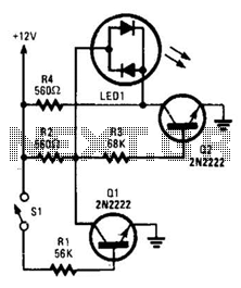
With switch SI open, base bias is supplied to transistor Q2 through a voltage divider formed by resistors R2 and R3, which activates the green element of the LED. This indicates that power is being supplied to the project....
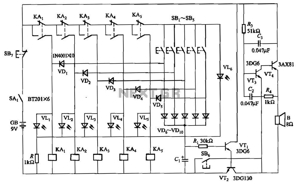
A relay-style circuit designed for a five electronic responder group. This circuit features self-locking capabilities, sound and light displays, time monitoring, and additional functions. The circuit includes a monitoring time button operated by the moderator. When this button is...
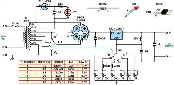
The following circuit illustrates a Battery Replacement Power Supply Circuit Diagram. This circuit is based on the LM317 integrated circuit. Features include the ability to replace... The Battery Replacement Power Supply Circuit utilizes the LM317 voltage regulator to provide a...

CMOS and PMOS cross interface circuit with PMOS integrated circuit providing high input impedance, allowing the input current to be negligible. The CMOS and PMOS interface circuit is illustrated in the accompanying figure. The CMOS and PMOS cross interface circuit...

The circuit depicted in Figure 3-157 is designed for motors with a capacity of no more than 11 kW, requiring precise stopping capabilities. Upon shutdown, contact KMi releases, and the motor stator windings are configured into a three-phase rectifier...