
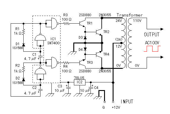
Discrete Voltage Inverter

The described circuit operates as a negative voltage generator using discrete components, specifically five n-p-n transistors. The essential components include transistors T1, T2, T3, T4, and T5, along with capacitors C1 and C2, resistors R4, R5, and R6, and a TTL clock signal. The operation begins with the clock signal oscillating at approximately 1 kHz, which is critical for the timing of the transistors' switching actions.
When the clock signal is high, T1 and T2 are activated, allowing capacitor C1 to charge from the supply voltage, UIN. This charging phase is crucial as it sets up the initial conditions for generating the negative voltage. The conduction of T5 during this period ensures that T3 and T4 remain off, preventing any premature discharge of the capacitors.
As the clock transitions to a low state, T5 is turned off, which triggers T3 and T4 to turn on through the pull-up resistor R6 and either R4 or R5. This switching action leads to the redistribution of charge between capacitors C1 and C2. Given that the positive terminal of C2 is grounded, this results in a negative voltage appearing at the negative terminal of C2 relative to ground.
The design requires that the high level of the clock input matches or exceeds the supply voltage, UIN, to ensure that T1 can effectively switch on. This condition is vital for the proper functioning of the circuit. The 1 kHz frequency is selected to achieve a duty cycle of 1:1, which is optimal for generating the desired negative voltage output. Adjustments to the duty cycle ratio can yield varying levels of negative voltage, but it is important to note that the output will always be lower than that produced with a 1:1 ratio. This circuit provides an efficient method for generating negative voltages without the need for integrated circuits, showcasing the utility of discrete transistor components in voltage regulation applications.The circuit in the diagram enables a negative voltage to be derived without the use of integrated circuits. Instead, it uses five n-p-n transistors that are driven by a 1 kHz (approx) TTL clock. When the clock input is high, transistors T1 and T2 link capacitor C1 to the supply voltage, UIN, which typically is 5 V.
During this process, transistor T5 conducts so that T3 and T4 are off. When the clock input is low, T5 is cut off, whereupon transistors T3 and T4 are switched on via pull-up resistor R6 and either R4 or R5. This results in the charge on C1 being shared between this capacitor and C2 Since the +ve terminal of C2 is at ground potential, its ve terminal must become negative w.
r. t. earth. The high level at the clock input must be of the same order as the positive input voltage, UIN, otherwise T1 cannot be switched on. The clock frequency should be around 1 kHz to ensure a duty cycle ratio of 1:1. Altering the ratio results in a different level of negative output voltage, but this is always smaller than that with a ratio of 1:1.
🔗 External reference
Related Circuits
The circuit utilizes one-half of a dual D flip-flop as an inverter. When the input signal decreases, the flip-flop resets, causing its Q output to increase. Conversely, when the input signal increases, the reset line is released, and the...
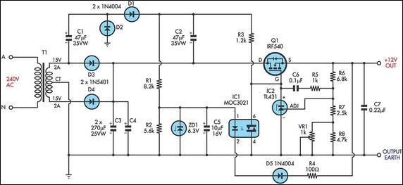
The circuit is a MOSFET-based linear voltage regulator capable of a voltage drop as low as 60mV at 1A. It utilizes a 15V-0-15V transformer and an IRF540 N-channel MOSFET (Q1) to provide a regulated 12V output. The gate drive...
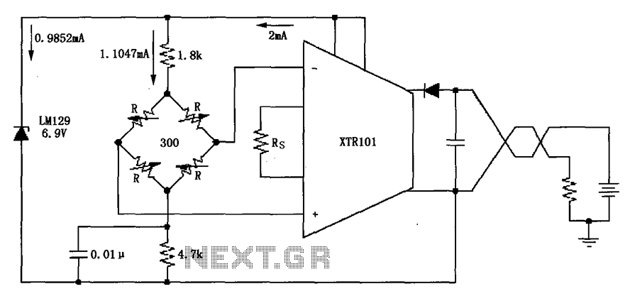
The circuit utilizes the LM129 voltage regulator to produce a 6.9V voltage reference, supplying a current of 1.0147mA from the 6.9V reference voltage to the bridge. The bridge may consist of varistor-type pressure sensors. The LM129 voltage regulator is a...
This 12 VDC to 240 VAC inverter circuit does not utilize specialized components, such as the toroidal transformer commonly found in many inverter circuits. The inverter circuit described is designed to convert a 12 VDC input into a 240 VAC...
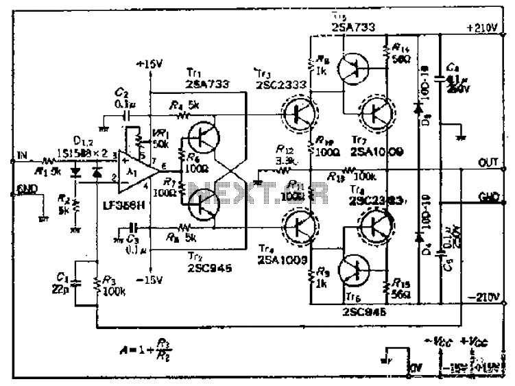
This amplifier circuit operates with an OP amplifier that is power-driven, which leads to the presence of floating voltage errors and necessitates a high-pressure booster for transistor protection. The circuit utilizes a mutual feedback configuration, connecting to the output...
The circuit utilizes an integrated circuit (IC) type multivibrator as the oscillator for alternating current, operating at approximately 60 Hz. The 7400 IC is employed for this purpose, although the 7404 IC can also be used. The oscillator signal...