
ESP Sound Impairment Monitor

The described circuit is a differential amplifier, which is a fundamental building block in analog electronics, particularly in signal processing applications. The primary function of this circuit is to amplify the difference between two input signals while rejecting any common-mode signals. This characteristic makes it particularly useful in environments where noise and interference are prevalent.
The circuit employs a variable resistor, designated as VR1, which allows for fine-tuning of the amplifier's offset. This adjustment is crucial for nullifying any inherent variations or offsets that may occur in the absence of distortion. By carefully setting VR1, the user can ensure that the output remains stable and accurate, even when the input signals are at their baseline levels.
The first stage of the amplifier is configured to operate as a differential input stage, typically utilizing operational amplifiers (op-amps). These op-amps are selected based on their performance characteristics, with the recommendation to utilize high-quality components from manufacturers such as Analog Devices or Burr-Brown for enhanced performance, particularly at higher frequencies. While standard op-amps may suffice for many applications, premium devices can provide improved bandwidth, lower noise, and better linearity, which are essential for high-fidelity signal processing.
Following the differential input stage, the second stage of the circuit is a high-gain amplifier. This stage is responsible for amplifying the residual signal output from the first stage to a level that is suitable for subsequent processing by rectifier and indicator circuits. The design of this stage must consider the gain requirements and the bandwidth to ensure that the amplified signal retains the integrity of the original input.
The circuit's layout should also incorporate appropriate power supply decoupling and grounding techniques to minimize noise and ensure stable operation. Additionally, the selection of passive components, such as resistors and capacitors, should be made with attention to tolerance and temperature coefficients to maintain performance across varying conditions.
Overall, this differential amplifier circuit is a versatile solution for applications requiring precise signal amplification with minimal distortion and noise, making it an essential component in various electronic systems.A differential amp used by the SIM, and it is a completely conventional circuit. This is adjustable by using VR1 to null out any normal variations that the amp might show when there is no distortion or other nastiness in evidence. The second stage is a high gain amplifier, and will amplify the residual signal to a level suitable for the rectifier and indicator circuits.
The opamp shown is adequate for most applications, but the use of a premium device from Analog Devices or Burr-Brown will improve performance, especially at high frequencies. This is not strictly necessary, because the operation of any amplifier protecti 🔗 External reference
Related Circuits
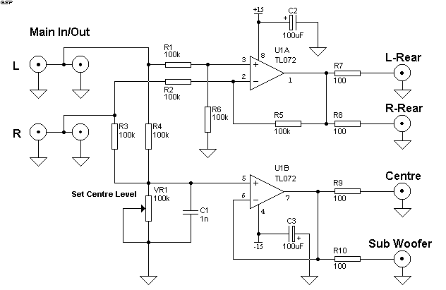
Simple Surround Sound Decoder. Introduction This surround-sound decoder is based on the Hafler principle, first discovered by David Hafler sometime in the early 1970s. The original idea. The simple surround sound decoder utilizes the Hafler principle to create an immersive...
This circuit can be utilized in a garden setting to detect unusual sounds or wildlife noises. It can also monitor sounds around a car parked in a remote location. The cable used for the setup can either be visible...
This is a relay circuit that detects the presence of sound to activate the relay. This sound-controlled relay can be utilized as a voice-operated switch or for controlling lights. The sound-activated relay circuit typically employs a microphone or a sound...

Creating a variable space in a small room can be enjoyable; however, designing an actuator to move a wall or room partition poses challenges. This can be achieved using an analog audio line delay. To implement a system that allows...
The structure and working principle of this circuit are fundamentally similar to the previous circuit, with some variations in the components used. The circuit is divided into seven bands, with center frequencies selected at 60 Hz, 150 Hz, 400...
Most sound card microphone inputs require a minimum signal level of at least 10 millivolts, but some older 8-bit cards need as much as 100 millivolts. The typical impedance of the PC sound card microphone input is in the...