
Spectrum monitor with memory function circuit

The input mixing circuit is depicted in Figure 4-64. The left and right channel input signals are received from the input terminals and mixed through resistances R1 and R2. After mixing, the signals are coupled to the isolation amplifier IC1-4. The values of R1 and R2 are chosen to minimize the impact on the degree of separation. The output from IC1-4 is amplified and split into two paths. One path passes through a coupling bar and a voltage doubler rectifier (VDi and rDz) followed by a filter capacitor (C3), which produces a DC voltage that reflects the intensity of the signal. This voltage is then fed to the base of transistor VTi, which amplifies the signal and controls the input signal strength to IC1-4 through the resistor VTzC-E, stabilizing the output level.
The second path includes the bandpass filter elements composed of IC1-L to IC1-3 and IC2-1 to IC2-4, which process the output voltage from the bandpass filter. The signal is then rectified through diodes D4 to D10 to obtain a DC voltage that reflects the strength of the band. To address the high turn-on voltage of silicon diodes, a dead zone elimination circuit is implemented, consisting of resistors Rg and Rose. A low-frequency germanium transistor is used to create a stable voltage drop of approximately 0.3V, effectively reducing the influence of the dead zone voltage associated with silicon diodes. This comprehensive approach ensures accurate signal processing and analysis, enhancing the circuit's overall performance in frequency component analysis.Structure and working principle of this circuit is basically the same as the previous circuit, but with some of the components used in the functional minor Ran o First show different bands of the circuit is divided into seven bands, the center frequency of 2.5 octave selection, respectively to 60Hz, 150Hz.400Hz, 1kHz, 2-5 "seven, 6kHz: and 15kHz; the second is the voltage comparator circuit using the LB1404 to replace a two op amp, comparator increases by 8 to 9 comparison, the display matrix consisting of 8 8 variants of 7 9; Third, before the addition of a bandpass filter input amplifier and automatic level control circuit, to overcome the large dark screen phenomenon signals the full screen and small signals. while the addition of a memory selection circuit controlled by the switch, then through the switch when being displayed spectrum is fixed, so that the frequency components of the signal strength and a careful analysis of the signal.
whole circuit consists of mixing the input signal amplification, automatic level control, electronic switches, scanning pulse distribution, the band-pass filter and the memory selection circuit and other components. o circuit as shown in Figure 4-64 input mixing circuit. left and right channel input signal from the input terminal, the mixed units resistance Rl, after mixing R2, coupled by the cl to ICI-4 for isolation amplifier o Rl, R2 larger value to reduce the impact on the degree of separation.
ICl.4 signal is amplified and divided into two, all the way through the coupling bar, after VDi ,, rDz voltage doubler rectifier and C3 filter, the resulting reflected signal intensity of dc voltage, the VTi Makati to the base, then amplified by the VTi control VTzC-E Q-resistance phase should control the input ICI-4 to the strength of the signal, thereby stabilizing the output level; the other way is added to Icl-L ~ lCl.3, IC2-1 ~ IC2-4 and 7 surrounding the band-pass filter element composed, for division processing the signal voltage output from the band pass filter, subject to rectifying diodes ,, D4 ~ VDio to get the letter reflect the band of the DC voltage signal strength. Since silicon diode turn-on voltage (saying dead) high, in order to overcome the shadow of the dead zone voltage response, the circuit is set dead zone elimination circuit, which consists of Rg and Rose composition, fb is the use of low-frequency germanium transistor eb drop between poles to form a better performance 0,3V stable voltage, in order to reduce the influence of the dead zone voltage silicon diodes.
orm action = "/ e / pl / doaction.php" method = "post" name = "saypl" id = "saypl" onsubmit = "return CheckPl (document.saypl)" spectrum displayed is fixed, for frequency component and a careful analysis of the signal strength of the signal. The whole circuit from the mixed input signal amplification, automatic level control, electronic switches, scanning pulse distribution, a bandpass filter and a memory selection circuit.
O circuit as shown in Figure 4-64 input mixing circuit. Left and right channel input signal from the input terminal, the mixed units resistance Rl, R2 after mixing, coupled by the cl to ICI-4 for isolation amplifier o Rl, R2 larger value to reduce the impact on the degree of separation. ICl.4 signal is amplified and divided into two, all the way through the bar coupling, VDi ,, rDz voltage doubler rectifier and C3 filter, the resulting reflected signal intensity of dc voltage, the VTi Makati to the base, amplified by the VTi and then ask the control VTzC-E-resistance phase should control the strength of the signal input to the ICI-4, thereby stabilizing the output level; the other way is added to Icl-L ~ lCl.3, IC2-1 IC2 ~ 7 bandpass filter 4, and the composition of the surrounding elements, as the division process.
By the signal voltage output from the band pass filter, subject to rectifying diodes ,, D4 ~ VDio to get the letter reflect the band of the DC voltage signal strength. Since silicon diode turn-on voltage (saying dead) high, in order to overcome the shadow of the dead zone voltage response, the circuit is set dead zone elimination circuit, which consists of Rg and f Rose composition, fb is the use of low-frequency germanium transistor eb inter-electrode voltage drop, form a better performance 0,3V voltage stability, to reduce the effect of the dead zone voltage silicon diodes.
Related Circuits
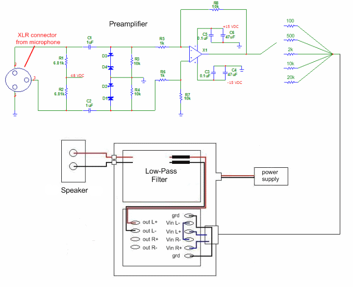
The XLR connector facilitates the connection of the microphone's output to the preamplifier circuit. This preamplifier was designed and constructed by Electrical Engineers using discrete components. The signal from the preamplifier is subsequently fed to the Maxim Class-D amplifier....

The Adjustable Timer circuit initiates timing upon activation. A green LED illuminates to indicate that timing is in progress. Once the designated time period elapses, the green LED turns off, the red LED activates, and an audible bleeper sounds....
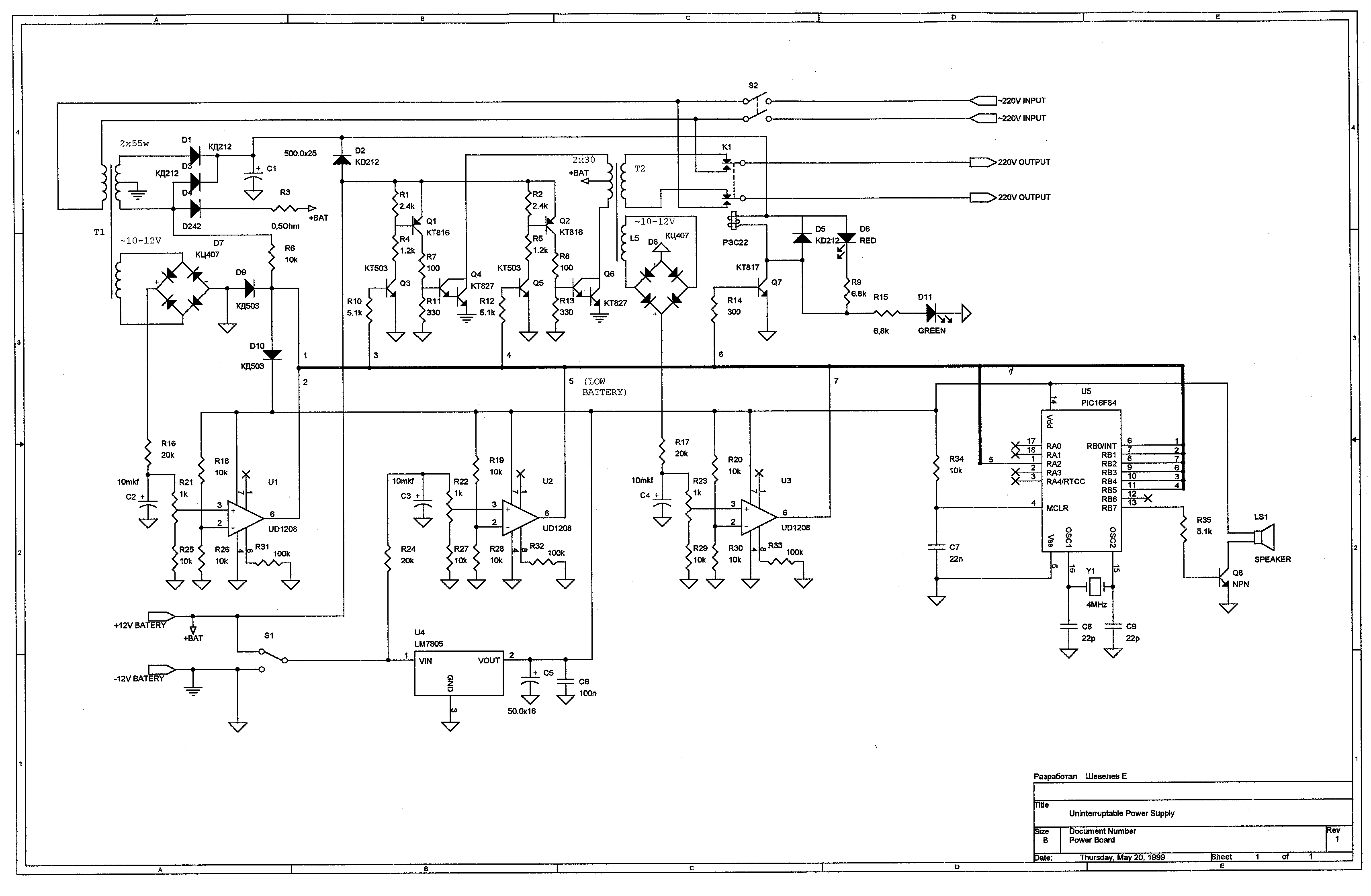
Full sine wave UPS information in English, along with detailed C language source code. English proficiency may be a concern, so caution is advised. A full sine wave Uninterruptible Power Supply (UPS) is designed to provide a stable and continuous...
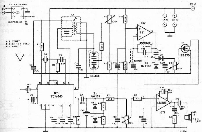
A simple FM CB radio receiver can be constructed using the electronic diagram provided. This FM CB radio receiver circuit utilizes a TCA440 integrated circuit and operates at an intermediate frequency of 455 kHz. The input filter is a...
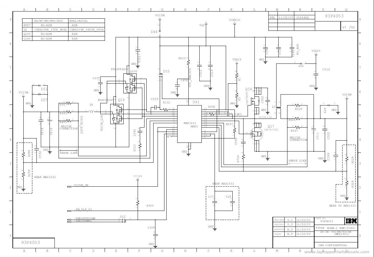
This is an IBM ThinkPad T40 power control circuit. This circuit is based on the MAX1631 IC, which is a multi-output, low-noise power supply. The IBM ThinkPad T40 power control circuit utilizes the MAX1631 integrated circuit (IC) to provide stable...
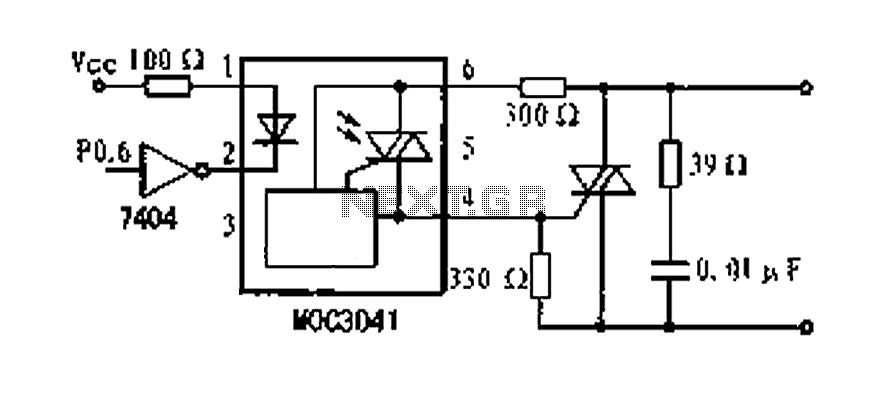
A dimming control circuit is implemented using a single-chip I/O port sinking method to control a thyristor switch for dimming functionality. The MOC3041 optocoupler features an internal zero-crossing detection circuit, allowing for effective control of the thyristor. This design...