
FAN7710 Ballast Control circuit design

The FAN7710 is a versatile integrated circuit specifically designed for driving compact fluorescent lamps (CFLs). Its architecture is optimized for high-voltage applications, allowing for efficient operation while maintaining a compact footprint. The internal circuitry of the FAN7710 includes features that facilitate the management of high-voltage stress, thereby enhancing the reliability and longevity of the lamp driver.
The preheating and ignition function is critical for the initial startup of the fluorescent lamp. By utilizing an external capacitor, users can customize the preheating duration, which is essential for prolonging the lifespan of the lamp. This feature minimizes thermal shock to the lamp's components during ignition, thereby reducing the likelihood of premature failure.
The internal active Zero-Voltage Switching (ZVS) control circuit is a significant advancement in ensuring efficient switching operation. This feature allows the FAN7710 to minimize electromagnetic interference (EMI) and improve overall energy efficiency by ensuring that the switch operates at zero voltage, thus reducing switching losses.
The conversion of the AC line input voltage (230 VAC at 50 Hz) to a high DC voltage (approximately 320V) is achieved through a rectification process. This high voltage is essential for the operation of the fluorescent lamp, which requires a substantial voltage to initiate and maintain the discharge process.
The startup resistor (R1) plays a pivotal role in the initial power-up sequence of the FAN7710. It provides the necessary biasing to kickstart the oscillation process within the IC. Once the oscillation begins, the charge pump circuit, comprising capacitors and diodes, efficiently supplies current to the VDD pin. This current is regulated via an internal 15-V shunt regulator, ensuring stable operation of the IC throughout its operational range.
Overall, the FAN7710 Ballast Control IC represents a robust solution for driving compact fluorescent lamps, combining efficiency, reliability, and user customization in a single integrated package. Its design is particularly suited for applications where cost-effectiveness and simplicity are paramount.Using the FAN7710 Ballast Control IC for Compact Fluorescent Lamps developed using Fairchild`s unique highvoltage process and system-in-package (SiP) concept can be designed a very simple low cost fluorescent lamp driver electronic project. The FAN7710 ballast control controls internal high-voltage stress and delivers 20W to the lamp at 320VDC vo
ltage. FAN7710 ballast control incorporates a preheating /ignition function, controlled by an user-selected external capacitor, to increase lamp life. The FAN7710 detects switch operation from after ignition-mode through an internal active Zero-Voltage Switching (ZVS) control circuit.
The AC line input voltage (230 VAC 50 Hz) is rectified to provide a bus voltage of approximately 320 volts DC. Startup resistor R1 supplies initial power to the FAN7710 IC. The IC begins to oscillate and the charge pump circuit consisting of C2, D2 and D7 supplies the current to the VDD pin, which gets regulated through the internal 15-V shunt regulator.
🔗 External reference
Related Circuits

Many microcontrollers or PICs have uncommitted digital-to-analog converter (DAC) outputs that can generate sine waves. However, these outputs typically have low resolution (8 to 10 bits), resulting in total harmonic distortion (THD) in the range of 1%. Alternatively, using...

This circuit illustrates the TDA1054 tone control stereo preamplifier circuit diagram. Features include the National Semiconductor LM35 integrated circuit, which utilizes semiconductor technology. The TDA1054 is a versatile integrated circuit designed for use in audio applications, particularly in tone control...
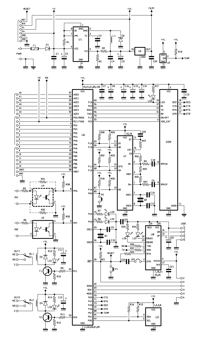
Utilizing the ATmega 2560, which serves as the core of the Arduino platform, a universal remote control with GSM capabilities has been developed. This device allows for the control of 2 inputs and 2 outputs, DTMF key functionality, gate...

To create the circuit, connect a switch as an input and an LED as an output to the Arduino. The components required include a switch, an LED, a 10kΩ resistor, a 470Ω resistor, a blue or yellow jumper wire,...

A low-cost, simple radio circuit schematic using an operational amplifier. This radio circuit diagram consists of a sensitive audio amplifier that receives strong signals. The presented radio circuit schematic utilizes an operational amplifier (op-amp) to create a cost-effective and straightforward...

Motor Bike Headlight Controller Circuit. This circuit automatically turns a motorcycle's headlight on and off, independently of both the light and ignition switches, provided the battery is fully charged. The first stage... The motorcycle headlight controller circuit is designed to...