
Flip-Flop Using CMOS NAND Gates

The described circuit utilizes two NAND gates or inverters to create a simple D-type flip-flop configuration with a push-button mechanism for toggling its state. Upon initial power-up, the output of the second gate (N2) is set to a high logic level (1), which keeps the output of the associated transistor (T2) in an off state. When the push-button is activated, it causes N2 to transition to a low logic level (0), resulting in T2 turning on and allowing current to flow.
The interconnection between the two gates (N1 and N2) is crucial as it ensures that the output of N1 is always the logical inverse of N2. This complementary behavior guarantees that the two transistors (T1 and T2) are never in the same state; one is always conducting while the other is off. This toggling action occurs with each press of the push-button, effectively allowing the circuit to function as a flip-flop.
In scenarios where output load is minimal, it is feasible to directly connect the outputs of N1 and N2 to external circuits, thereby eliminating the need for the transistors. However, caution is advised since the 4000 series CMOS devices have a limitation of sourcing or sinking a maximum of 0.5 mA at a supply voltage of 5 V. Therefore, implementing open-collector transistor buffers is recommended for enhanced reliability and safety.
This configuration is particularly advantageous for designers who may have surplus unused gates in their circuit designs, as it negates the necessity of incorporating a dedicated flip-flop integrated circuit. It is also critical to connect the inputs of any unused CMOS gates to either the positive supply or ground to prevent floating inputs, which can lead to unpredictable behavior.
The circuit operates effectively over a supply voltage range of 3 V to 15 V, with the current consumption varying between 0.2 mA and 5 mA when there is no load present. This flexibility in supply voltage and low current draw makes the circuit suitable for various low-power applications, ensuring efficient operation within the specified parameters.Using just two NAND or inverter gates its possible to build a D type (or toggle`)‚ip-‚op with a push-button input. At power-up the output of gate N2 is at a logical 1`, ensuring that transistor T2 is switched off. When the push-button is pressed the output of N2 changes to a logical 0` and transistor T2 conducts. The coupling between N1 and N 2 ensures that the output of N1 will always be the inverse of N2 so T1 and T2 will always be in opposite states and will flip each time the push-button is pressed. In some cases it is possible to omit T1 and T2 and use the outputs of N2 and N1 to drive external circuitry directly but only if the loading on these outputs is low enough.
The 4000 series CMOS family can source/sink a maximum of 0. 5mA (at 5 V) so for the sake of safety its best to use these open-collector congured transistor buffers. This circuit is particularly useful if you have some unused gates left over in a circuit design, avoiding the need to add a dedicated flip-flop IC.
It is worth remembering that all other unused CMOS gates must have their inputs connected to either the positive or ground rail. The supply voltage can be in the range 3 V to 15 V for CMOS ICs and the current taken by this circuit is between 0.
2 mA and 5 mA (no load). 🔗 External reference
Related Circuits
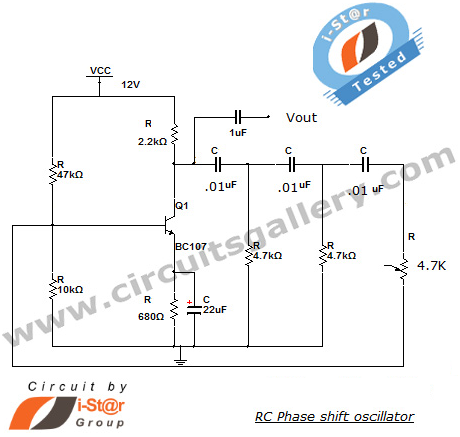
This section introduces a transistor oscillator circuit known as the RC Phase Shift Oscillator. An oscillator is an electronic circuit that functions as a sine wave generator, requiring only a DC power supply. It is commonly used in variable...
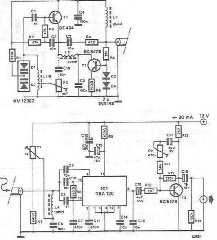
The tuning stage of this long-wave and medium-wave radio receiver also functions as an active antenna, which can be optimally positioned for the best reception. The circuit is completely independent from the receiver, which includes a demodulator that provides...
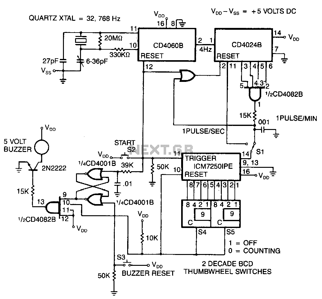
The time base is initially selected with switch S1 set for either seconds or minutes. Subsequently, values from 0 to 99 are chosen using the two thumbwheel switches S4 and S5. Finally, pressing switch S2 starts the timer. At...

The circuit diagram of an FM transmitter utilizes the IC UPC1651, which is a wideband UHF Silicon MMIC amplifier. This integrated circuit features a broad frequency response of up to 1200 MHz and a power gain of up to...
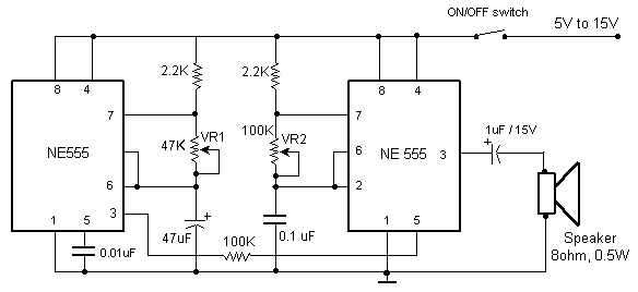
The primary components of this doorbell circuit include two NE555 timer integrated circuits (ICs). When the switch S1 is pressed momentarily, the loudspeaker emits a bell tone for the duration determined by the time period of the monostable multivibrator...
Using the superposition theorem, it is necessary to determine the current at all three nodes of the circuit. The current from the source, denoted as i_1, represents the current through V1 when other voltage sources are shorted out, in...