
Frequency comparator II

These signals are latched by IC5 at the end of each period, triggered by a latch signal from IC6e. When the two frequencies are within a tolerance of ±0.6%, the least significant bits (LSBs) of the counter IC2 are decoded and latched by IC7, which then displays the values on the LEDs. IC6c resets the counter following the data latching process.
The circuit operates by first establishing a reference frequency through a phase-locked loop (PLL) and a frequency divider. This reference frequency is crucial for accurate measurement and comparison against the incoming signal. The division of the measured frequency allows for a manageable range of values for the counter IC2, which is designed to handle up to 1024 pulses.
The use of latches (IC4a, IC4b, and IC5) ensures that the system can reliably capture and hold the state of the frequency measurements at specific intervals, allowing for a stable output on the LED display. The tolerance of ±0.6% is a critical design feature, ensuring that minor fluctuations in frequency do not result in erroneous readings. The decoding and display of the LSBs further enhance the usability of the circuit by providing a precise visual representation of the measured frequencies.
The reset function provided by IC6c is essential for preparing the counter for subsequent measurements, ensuring that each measurement cycle starts from a known state. Overall, the circuit is designed for precise frequency measurement and display, making it suitable for applications requiring accurate and real-time frequency analysis.The circuit provides unambiguous LED + or - bar readout with steps of 0.1%. The reference frequency is multiplied by the PLLIC1 and divider IC9 to output 64 ? F (ref) and this is then gated by dividing F (measure) by 32 in IC8 thus is F (ref) = (measure) then IC2 counts 1024 pulses. Should the count be more than 1031 than the latch IC4c/IC4a is set to indicate count too high (F (measure) F (ref)) and if the count is less than 1017 then IC3/IC4b indicate count too low (F (measure) F (ref).
These signals are latched by IC5 at the end of each period by the latch signal from IC6e. When the two frequencies are within + or - 0.6% the LSB's of the counter IC2 are decoded and latched by IC7 and displayed on LED's IC6c resets the counter after latching the data.
Related Circuits
%2Busing%2Bop%2Bamp%2B741%2Bic%2B.png)
A zero crossing detector (ZCD) is a voltage comparator that switches its output between +Vsat and -Vsat (where Vsat is the saturation voltage, approximately 14V) when the input crosses the zero reference voltage. Comparators are fundamental operational amplifier circuits...
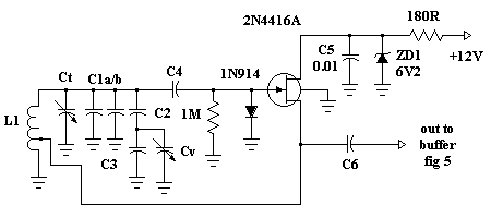
The RF design and construction of radio frequency oscillators. Radio frequency (RF) oscillators are essential components in various electronic systems, generating signals at specific frequencies used for communication, signal processing, and other applications. The design of RF oscillators involves several...

The beat frequency oscillator (BFO) is essential for receiving continuous wave (CW) signals. Since CW signals lack an audio modulation component, it is necessary to introduce one. The functions of the RF amplifier, mixer, local oscillator, and IF amplifier...
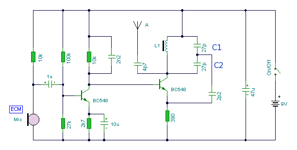
This result places the oscillator within the UK FM Band, which ranges from 87.5 to 108 MHz. If L1 is equipped with an adjustable ferrite core, its inductance can be modified, allowing for fine tuning. If L1 consists of...
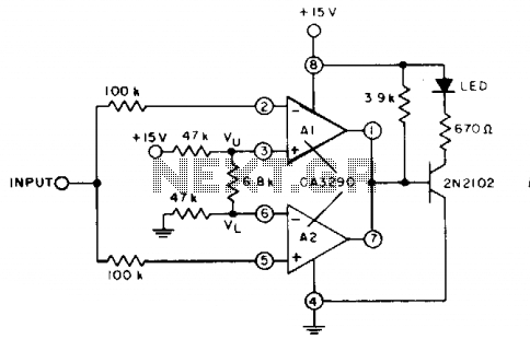
The circuit utilizes both halves of the CA3290 BiMOS dual voltage comparator. The LED will be activated whenever the input signal is above the lower limit (VL) but below the upper limit (Vy). The circuit design employs the CA3290 BiMOS...

A discrete oscillator circuit illustrated in the schematic diagram below is a variable duty cycle and variable frequency oscillator, which can be utilized to generate various output waveforms. The discrete oscillator circuit is designed to produce oscillations with adjustable frequency...