
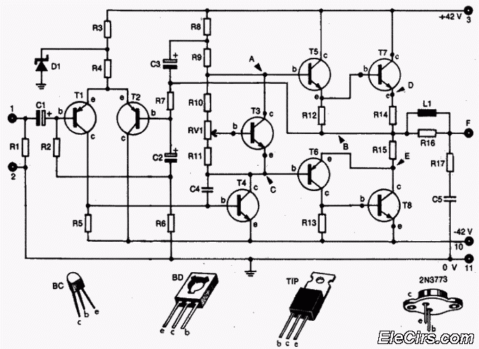
Headphone electrostatic JFET Amplifier

Because the amp is totally DC coupled from input to output, drift in the input stage is a bad idea. Since the first two stages run in current mode, the JFET input is more linear than a pair of bipolar transistors. Dual transistors all on one wafer suitable for audio use are hard to find these days.
The approximate voltage gain of this stage is 5. But it really runs in current mode. The unit was designed to work equally well in both balanced and unbalanced mode. For single-ended signals, ground either the + or - input and apply signal to the other. The much higher impedance of the JFET works better when one side is grounded for unbalanced inputs.
The second stage starts with a constant current source. The current source feeds a common base amplifier. The common base amplifier feeds a modified Vbe multiplier. Its the most linear way of translating the voltage down to the bottom rail. The voltage gain of this section is about 4. The basic idea of the first two stages is to supply the third stage with a very fast low impedance drive signal that is referenced to the bottom rail.
The current sources in the second stage supply 2 mA each. With no signal, the FETs take 1 mA, leaving 1 mA going through the common base amplifier into the bottom transistor (which is wired as a vbe multiplier). This generates the 13 volts (referenced to - rail) necessary to properly bias the 3rd stage. The bottom transistor acts like a zener diode in series with a resistor, except a lot less noisy.
The third stage is another differential amplifier feeding another common base amplifier. The simple differential amplifier has a voltage gain of about 100. The common base amplifiers are used to reduce the miller effect on the differential pair. Since the miller effect depends on both gain and output voltage swing, reducing the output voltage swing of the bottom differential transistors significantly improves the speed of this circuit.
The fourth stage is an emitter follower driven by a constant current source (gain = 0.99). This output stage dissipates 12 watts total (3 watts per transistor x 4 transistors). The main design goal was low output impedance. This amp has a 25 ohm output impedance (actually a little less with feedback) resulting in a much more extended high end. The slew rate of the solid state amp is more than 5 times that of the tube amp.
For the output stage, each 2SC3675 sources or sinks 9 mA at a quiescent output voltage of zero volts referenced to ground. For the driver stage, each 2SC3675 sinks 1.1 mA, resulting in 1 VDC at the collector (referenced to ground). The bases of the 2SC2705s sit at about 16 volts (referenced to - rail). The overall open loop gain of the amplifier is about 2000, but feedback reduces it to 1000. Even without any feedback of any kind the total harmonic distortion of the amp is still under 0.02%. The unit uses an unregulated power supply. Given the stiffness of the capacitors, and the fact that the amplifier is pure class A, there is absolutely no fluctuation in voltage when signal is supplied. A regulated design is also available. The 2SC3675 and 2SA1968 are mounted on heatsinks. The transformer is a Thordarson 24R22U (Allied # 704-0952). The ±15 volt supply is an encapsulated fully regulated power supply brick from Sola Linear (Allied part number 921-9215), which retails for $117. A 60 mA version is used, but that is overkill, because the total current drain is about 12 mA for both channels. It is noted that switching supplies are not utilized in audio applications whenever possible.
The amplifier's design emphasizes low output impedance and high linearity, making it suitable for high-fidelity audio applications. The use of JFETs in the input stage aids in maintaining low noise and high input impedance, which is critical for audio signal integrity. The architecture of the amplifier, with its multiple stages of current and voltage control, allows for a significant reduction in distortion and an extended frequency response compared to traditional tube amplifiers. The careful selection of components, such as the 2SC3675 and 2SA1968 transistors, and the implementation of a robust power supply, further enhance the amplifier's performance, ensuring reliability and consistency in sound quality. The overall design philosophy prioritizes audio fidelity, speed, and efficiency, making it a compelling choice for audiophiles.The amplifier operates primarily in the current domain. The first stage is a voltage controlled current sink. The second stage is a current-controlled voltage source. The fourth stage is a constant current sink. The main advantage of current domain amplifiers is speed. Standard voltage gain amplifiers with lots of gain are affected by the Miller Effect which prohibits extended frequency response. This solid state amp is so much better than my tube amp that I no longer listen to it. I'm not a solid state snob; it's just plain better. The people who have listened to this amplifier (some of whom were giants in the industry in their day) love it, much more than my tube amp.
I love it too. I can't stop listening to it. The tube amp has moved into a secondary position in my listening rack. The first stage is a differential amplifier with feedback directly from the output stage. It works equally well with both balanced and unbalanced audio input sources. The step attenuators from Goldpoint make good volume controls for this stage. The JFET device is a dual JFET all on one wafer. It is known for extremely low noise and excellent matching, and is used in a number of expensive designs, such as the Nelson Pass amplifiers. Because the amp is totally DC coupled from input to output, drift in the input stage is a bad idea. Since the first two stages run in current mode, the JFET input is more linear than a pair of bipolar transistors.
Dual transistors all on one wafer suitable for audio use are hard to find these days. The approximate voltage gain of this stage is 5. But it really runs in current mode. The unit was designed to work equally well in both balanced and unbalanced mode. For single-ended signals, ground either the + or - input and apply signal to the other. The much higher impedance of the JFET works better when one side is grounded for unbalanced inputs. The second stage starts with a constant current source. The current source feeds a common base amplifier. The common base amplifier feeds a modified Vbe multiplier. I believe a famous designer is now calling this circuit a current tunnel. Its the most linear way of translating the voltage down to the bottom rail. The voltage gain of this section is about 4. The basic idea of the first two stages is to supply the third stage with a very fast low impedance drive signal that is referenced to the bottom rail. The current sources in the second stage supply 2 mA each. With no signal, the FETs take 1 mA, leaving 1 mA going through the common base amplifier into the bottom transistor (which is wired as a vbe multiplier).
This generates the 13 volts (referenced to - rail) necessary to properly bias the 3rd stage. The bottom transistor acts like a zener diode in series with a resistor, except a lot less noisy. The third stage is another differential amplifier feeding another common base amplifier. The simple differential amplifier has a voltage gain of about 100. The common base amplifiers are used to reduce the miller effect on the differential pair. Since the miller effect depends on both gain and output voltage swing, reducing the output voltage swing of the bottom differential transistors significantly improves the speed of this circuit. The fourth stage is an emitter follower driven by a constant current source (gain = 0.99). This output stage dissipates 12 watts total (3 watts per transistor x 4 transistors). The main design goal was low output impedance. For example, my electrostatic tube amp has a 50K load resistor and thus has a 50k output impedance. This amp has a 25 ohm output impedance (actually a little less with feedback) The result is a much more extended high end.
The slew rate of the solid state amp is more than 5 times that of the tube amp. For the output stage, each 2SC3675 sources or sinks 9 mA at a quiescent output voltage of zero volts referenced to ground. For the driver stage, each 2SC3675 sinks 1.1 mA, resulting in 1 VDC at the collector (referenced to ground).
The bases of the 2SC2705s sit at about 16 volts (referenced to - rail). The overall open loop gain of the amplifier is about 2000, but feedback reduces it to 1000. Even without any feedback of any kind the total harmonic distortion of the amp is still under .02%. My first prototype, the unit in the pictures, uses an unregulated power supply. Given the stiffness of the capacitors, and the fact that the amplifier is pure class A, there is absolutely no fluctuation in voltage when signal is supplied. Of course, a regulated supply is always better. A regulated design is shown above. The 2SC3675 and 2SA1968 are mounted on heatsinks (the small tab ones are fine). The transformer is a Thordarson 24R22U (Allied # 704-0952). Adjust the pot to get 580VDC for the bias voltage. The ±15 volt supply is an encapsulated fully regulated power supply brick from Sola Linear (Allied part number 921-9215), which retails for $117.
I used a 60 mA version, but thats overkill, because the total current drain is about 12 mA for both channels. Lots of companies make these. It's the black brick in the picture. It is NOT a switching supply. I do not use switchers in audio stuff if I can possibly help it. 🔗 External reference
Related Circuits
Audio Amplifier with output power of either 100W or 130W. The output configuration can accommodate 2 transistors for 90W output or 4 transistors for 130W output. The PCB layout utilizes T3 on the heatsink. The component reference and values...
This design utilizes a well-established circuit topology for the power amplifier, employing a single-rail supply of approximately 60V and capacitor coupling for the speaker(s). The benefits for a guitar amplifier include a straightforward circuitry design, even for relatively high...
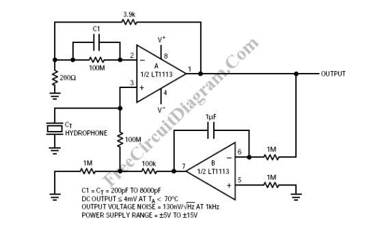
A hydrophone is similar to a microphone, but it is specifically designed for underwater environments. While a hydrophone can also capture sound in air, its sensitivity is reduced because its mechanical-acoustical properties are tailored to match the acoustic impedance...
A unit that is often very useful for isolating two stages in sound circuits. This circuit includes an amplification unit with a gain of X1. Total negative feedback is not employed; instead, only local feedback is used, resulting in...
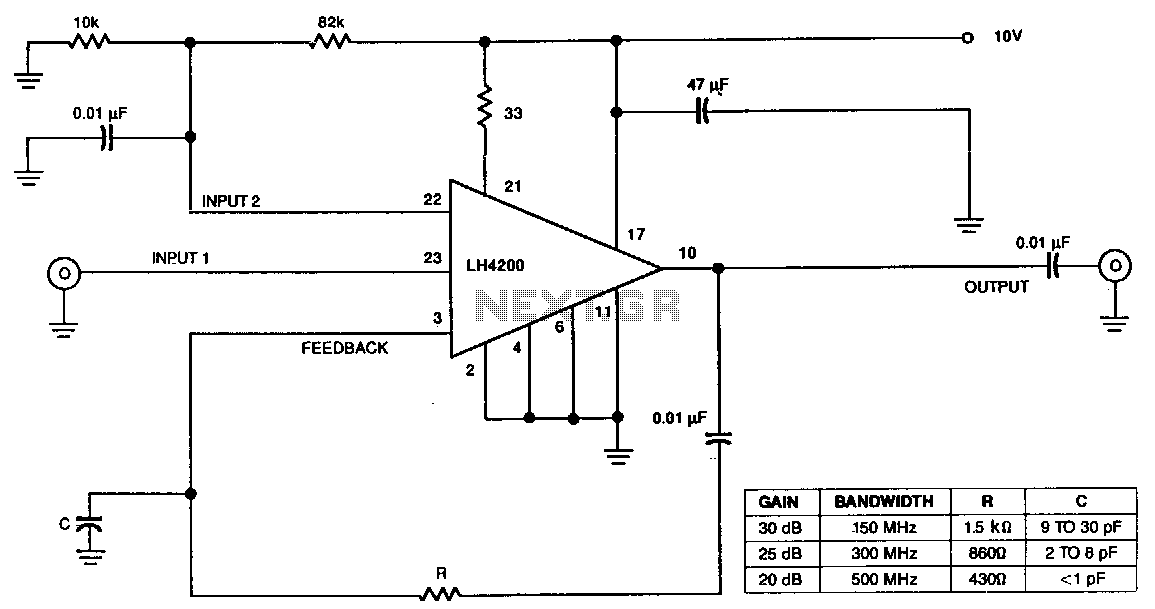
The amplifier's input stage features a dual-gate GaAs FET, which offers low input capacitance and high transconductance. The first input accepts the signal, while the second input regulates the amplifier's gain. Additionally, there is a third input for series...
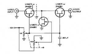
A variable gain amplifier controlled by voltage, functioning as a video amplifier. It utilizes three Field Effect Transistors (FETs) of type U1897E, which can be substituted with 2N4091. The described variable gain amplifier is designed to adjust its gain based...