
High voltage stabilizing circuit diagram composed of optocouplers
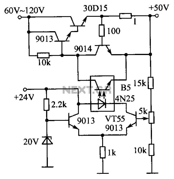
The described circuit operates with a focus on maintaining stable output voltage levels through feedback mechanisms involving various components. The use of a driving transistor with a higher breakdown voltage, such as the 9013, is critical for ensuring reliable operation under higher voltage conditions. The transistor VT55 plays a pivotal role in the circuit's performance as it regulates the biasing conditions.
When the output voltage increases, the forward current through the light-emitting diode (LED) also rises. This increase in current is significant as it affects the voltage across the photodiode, which is a key component in the feedback loop of the circuit. The reduction in voltage across the photodiode leads to a decrease in the biasing current for the regulator. This action effectively reduces the junction resistance within the regulator, which in turn causes the output voltage to decrease.
The feedback mechanism is essential for ensuring that the output voltage remains stable despite fluctuations in load conditions or input voltage variations. If the output voltage begins to rise excessively, the circuit automatically compensates by adjusting the biasing conditions, thereby preventing overvoltage situations. This self-regulating behavior is crucial for applications requiring consistent voltage levels, such as in power supply circuits or LED drivers.
Overall, the circuit exemplifies a robust design that utilizes feedback from the LED and photodiode to maintain output stability, ensuring reliable operation across varying conditions. The careful selection of components, such as the high breakdown voltage transistor and the configuration of the feedback loop, contributes to the overall effectiveness of the circuit in achieving its intended performance objectives. Circuit is shown. Normal driving transistor would need a higher breakdown voltage transistor (FIG driving tube 9013). When the output voltage increases, VT55 bias increases, B5 light emitting diode forward current increases, the voltage between the photodiode decreases, the regulator be biased to reduce junction resistance increases and the output voltage decreases ; on the contrary, the output voltage increases, thereby maintaining a stable output voltage.
Related Circuits
A circuit designed to operate within a frequency range with an accuracy greater than 2% for generating Bode plots. It converts two sine waves into a square wave, taking into account the overlap relative to the total input wave...
The quartz crystal oscillator circuit is highly advantageous in terms of frequency stability. Even the Voltage-Controlled Crystal Oscillator (VCXO) circuit, which allows for significant frequency changes, typically experiences only about a 1% variation. However, the linear range of control...
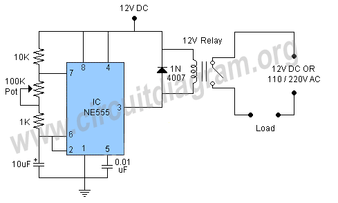
In this circuit, the 555 Timer IC is configured as an astable multivibrator, and a 12-volt relay is operated through pin 3 of the IC. The IC generates continuous pulses at pin 3, which activate and deactivate the relay,...

This document outlines the restoration of an antique AM/FM Granco 720 radio. It explores the design of the AM and FM receivers, detailing the alignment of these receivers, discussing repairs, and evaluating the radio's performance. The restoration of antique...
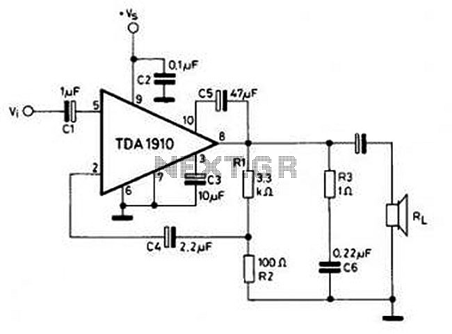
This circuit is simple and inexpensive, which is its primary advantage. Although the output power is not high, the audio quality is good due to the TDA1910's very low noise feature. This circuit is suitable for use as a...

A CMOS 4001 or a CMOS 4011 can be utilized in this circuit, as both contain four two-input gates. The inputs of each gate are connected together, allowing them to function as simple inverters. This means that when both...
Warning: include(partials/cookie-banner.php): Failed to open stream: Permission denied in /var/www/html/nextgr/view-circuit.php on line 713
Warning: include(): Failed opening 'partials/cookie-banner.php' for inclusion (include_path='.:/usr/share/php') in /var/www/html/nextgr/view-circuit.php on line 713