
Inductorless 3-5 Volts Converter

The charge pump circuit described utilizes a configuration that allows for flexible output voltage regulation. The MAX660 charge pump IC serves as the primary component, leveraging its internal oscillator to facilitate the transfer of charge between capacitors. The operation begins with the oscillator generating a frequency of 45 kHz, which is instrumental in moving charge from C1 to C2. This movement is critical for achieving the desired output voltage.
In this circuit, the feedback mechanism plays a vital role. The output voltage is monitored through pin 3 of the MAX921 comparator. When the feedback voltage surpasses the set threshold of 1.18 V, the comparator's output switches high, which effectively disables the oscillator through transistor T1. This feedback loop ensures that the output voltage remains stable and within the desired range.
The design incorporates a zero-hysteresis setting for the comparator, which is suitable for applications where precise voltage regulation is required without the need for delay in switching. The oscillator's brief operation, generating two cycles before being turned off, allows for fine control over the output voltage, preventing overshoot beyond the target level.
Output ripple is a critical consideration in this design. It is influenced by factors such as the input voltage, load current, and the characteristics of capacitor C1. Implementing a series resistor can help mitigate ripple but may reduce overall efficiency. The equivalent series resistance (ESR) of C1 also affects performance; lower capacitance values can lead to reduced charge transfer to C2, thus minimizing voltage fluctuations at the output.
In conclusion, this charge pump circuit effectively demonstrates how a comparator and transistor can be utilized to achieve regulated output voltages, allowing for versatility in applications requiring specific voltage levels. By carefully managing the components and their interactions, a reliable and efficient voltage regulation system can be established.By configuring a comparator and a transistor to control the oscillator in a charge pump circuit, you enable the pump to generate a regulated output of in principle any desired value. Charge pump ICs can either invert or double an input voltage (for example, 3 V to 3 V or 3 V to 6 V).
The charge pump itself does not regulate the output voltage a nd one running off 3 V is not normally capable of generating intermediate output voltage levels like 5 V. However, by adding a comparator and a reference device, you can create arbitrary output levels like 5 V and regulate them as well.
Charge pump IC1 (a MAX660) has an internal oscillator whose 45 kHz operation transfers charge from C1 to C2, causing the regulated output to rise. When the feedback voltage (pin 3 of IC2) exceeds 1. 18 V, the output of comparator IC2 (a MAX921) goes high, turning off the oscillator via T1. The comparator hysteresis (easily added on IC2) is zero here simply because no hysteresis is required in the control loop.
The oscillator when enabled generates two cycles, which is sufficient to drive VOUT slightly above the desired level. Next, the feedback turns the oscillator off again. The resulting output ripple will depend mainly on the input voltage and the output load current. Output ripple may be reduced at the expense of circuit efficiency by adding a small resistor (say, 1 ) in series with C1.
You`ll find that ripple also depends on the value and ESR associated with C1 - smaller values of C1 transfer less charge to C2, producing smaller jumps in V OUT. 🔗 External reference
Related Circuits
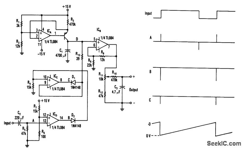
When the input transitions from low to high, a narrow positive pulse is generated at point A. This pulse results in a -13 V level at point B, which causes diode D2 to turn off. Consequently, the V+ voltage...
This project originated from an interest in a new form of radio transmission known as Digital Radio Mondial (DRM). The Digital Radio Mondial (DRM) is a revolutionary digital broadcasting technology designed for AM and FM radio. It provides enhanced audio...
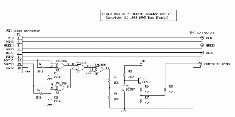
First circuit is for connecting VGA card to video projector or a monitor which accept VGA card frequencies and has RGB + Composite sync input. This circuit has been successfully used with Electrohome Projection Systems ECP 4100 data and...

This voltage-to-frequency converter (VFC) circuit utilizes a 555 integrated circuit (IC) and a 741 operational amplifier (op-amp) as its primary components. The circuit is capable of generating oscillations of up to 20 kHz. The voltage-to-frequency converter circuit is designed to...
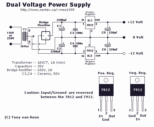
This circuit is a dual voltage regulated power supply, +12, -12, 0 volt. It uses the 7812 and 7912 regulators. You need a 18VCT, 1A transformer at input. More: Caution: Input / Ground are reversed between the 7812 and...
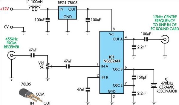
The signals below 550 kHz include maritime mobile, distress signals, radio beacons, aircraft weather information, European Longwave-AM broadcasts, and point-to-point communications. A low-frequency converter transforms the 10 to 500 kHz LW range into a 1010 to 1550 kHz MW...