
Joule Thief Circuit Explanations

The Joule thief circuit is a minimalist boost converter designed to extract energy from low-voltage sources, such as depleted batteries. This circuit is particularly effective for powering small electronic devices, utilizing components like a transistor, a resistor, an inductor, and a diode to achieve its operation.
The fundamental operation of the Joule thief involves the use of an inductor to store energy when the transistor is in the off state and then releasing that energy to the load when the transistor is turned on. The circuit typically comprises a NPN transistor (such as the 2N3904), which acts as a switch. When the circuit is powered, a small current flows through the base resistor, turning the transistor on and allowing current to flow through the inductor.
As the inductor stores energy, the magnetic field builds up. When the transistor is turned off, the collapsing magnetic field induces a voltage across the inductor, which is significantly higher than the original input voltage. This induced voltage is then rectified by the diode and can be used to power a load, such as an LED.
The circuit can be visually represented with the following components:
- A power source (typically a single-cell battery),
- A NPN transistor connected to the base via a resistor,
- An inductor connected in series with the collector of the transistor,
- A diode connected in parallel with the load to prevent reverse current,
- A load, such as an LED, connected to the output.
The Joule thief circuit is notable for its simplicity and efficiency, allowing it to operate with voltages as low as 0.5V. It is a popular project for electronics enthusiasts and serves as an educational tool for understanding basic concepts of inductive energy storage and boost conversion principles. Videos and circuit diagrams often accompany tutorials to provide visual aids, enhancing comprehension of the circuit's functionality and construction.Joule theif circuit and videos with circuit diagrams and explanations. 🔗 External reference
Related Circuits
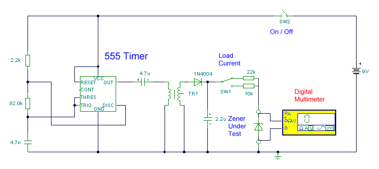
This circuit utilizes a single 555 Timer IC along with a small transformer to generate high voltage for testing zener diodes with voltage ratings up to 50VDC. The 555 timer operates in astable mode, with the output from pin...
This project is a successful vacuum tube amplifier utilizing a 6V6GT output pentode configured in triode mode, producing approximately 4.5 watts of output power. The design features a single-ended audio amplifier with a resistive input network, a driver stage,...

The schematic closely resembles the one found in the CPLD Development Board Tutorial, as it is essentially the same board with a minor addition. The new components are located in the lower right corner, including eight DIP switches, a...
This process can be simplified by utilizing a display kit from PJRC, which includes the appropriate firmware installed on the display, a functioning pushbutton board, and the necessary cables. The PJRC display features a 4-pin connector compatible with the...
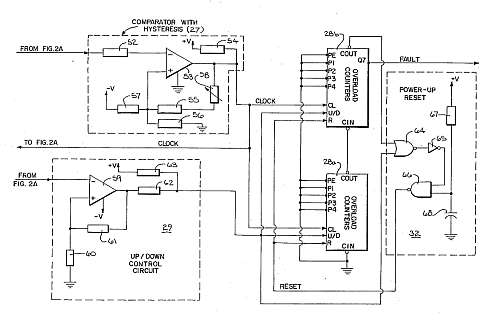
This motor overload circuit allows for short-term overdriving of a system, which is dependent on heat buildup. An overload detection circuit safeguards the motor against currents exceeding the rated current for specific exposure durations. The permissible exposure times are...
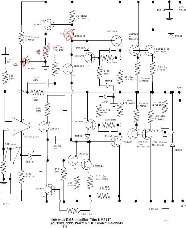
This is a 100-watt basic power amplifier designed to be relatively easy to build at a reasonable cost. It offers better performance, or musical quality, than the standard STK module amplifiers commonly found in mass-market stereo receivers. The design...