
Logic Probe with Pulse Indicator Circuit

The logic probe circuit is designed to provide visual feedback on digital signal levels, making it a valuable tool for troubleshooting and testing logic circuits. The use of a CMOS IC allows for a wide operating voltage range, accommodating various digital systems. The configuration ensures that the logic probe does not interfere with the circuit under test, thanks to its high-impedance state when no signal is present.
The buffer stage (IC1a) plays a crucial role in isolating the logic probe from the circuit, ensuring accurate readings without loading the tested circuit. The oscillation of IC1a when disconnected is a useful feature, as it provides an indication of the probe's operational status.
The potential divider formed by the two 1kΩ resistors is essential for determining the LED operation. In a high-impedance state, the output remains at half the supply voltage, which keeps the LEDs off. When a High or Low signal is detected, the corresponding LED illuminates, providing immediate visual feedback. The dim illumination of the LEDs in response to fast clock signals indicates the presence of pulsing signals, which can help in diagnosing signal integrity issues.
The monostable oscillator configuration created by IC1b and IC1c introduces a time delay, allowing the logic probe to filter out rapid fluctuations in the input signal. The timing components, specifically the 100nF capacitor and the 4.7MΩ resistor, set the duration of the output pulse, effectively stabilizing the LED indication in the presence of noisy or fast-changing signals.
Finally, IC1d's role as a buffer for the pulsing LED ensures that the output is capable of driving the LED without affecting the performance of the preceding stages. This design not only enhances the reliability of the logic probe but also improves its usability in various testing scenarios, making it an essential tool for electronics engineers and technicians.This is a circuit diagram for logic probe that is based on single CMOS IC. This logic probe shows three logic condition, High, Low, and Pulsing. Ind addition, there is no LED`s will glow if the probe input is neither hi or lo (the high impedance state of tri-output logic IC`s). This is the configuration of figure the circuit; This logic probe usin g power from the logic circuit under test; CMOS IC enables logic circuit is used to test using voltages from 3 to 15 volts. IC1a is used as a buffer with a difference. Under no input, i. e. the gate will oscillate due to feedback from the 2M2 resistor since the probe not connected to circuit.
IC1a output voltage is approximately half from supply voltage. The Hi and Lo logic indicator LED`s are connected to a potential divider. This potential divider consist of two 1K resistors. When there is no input, junction voltage is half supply voltage or high impedance no LED`s will glow. IC1a will rest in a permanent state because of Hi or Lo logic condition. This is indicated by either the Hi or Lo LED illuminating. Hi and Lo LEDs will light dimly with a fast oscillator or clock signal. This is the reason for IC1b and IC1c. These two gates form a mono stable oscillator, 100nF capacitor and 4M7 resistors determine the time constant.
This is effectively slowed using clock signal as the mono stable is continually triggered and retriggered. IC1d works like a buffer to drive the pulsing LED. 🔗 External reference
Related Circuits
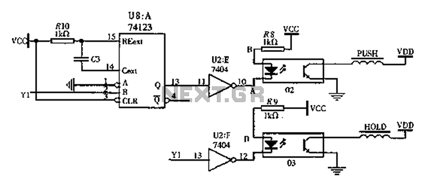
The FIG switching solenoid driver circuit utilizes the 74123 device chip (U8) and solid-state relays (02, 03). The switching electromagnet coil is referred to as the PUSH coil, while the HOL is maintained at a power supply voltage (VDD)...

This circuit was designed by Lazar Pancic from Yugoslavia. A typical PC sound card includes a microphone input, speaker output, and occasionally line inputs and outputs. The microphone input is specifically tailored for dynamic microphones with an impedance range...
This post presents an interesting topic about switching power supply circuit diagrams for those who wish to learn more. A switching power supply is a type of power supply that uses a switching regulator to convert electrical power efficiently. Unlike...
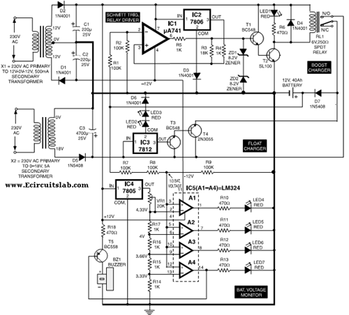
This circuit illustrates the use of the 7806 IC in an automatic battery charger circuit diagram. It is designed for a car battery with an approximate rating of 40 Ah. The automatic battery charger circuit utilizing the 7806 integrated circuit...
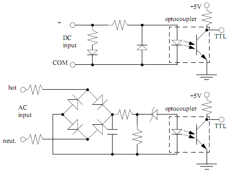
PLC input cards typically do not provide power, necessitating an external power supply for inputs and sensors. An example of an input card and a ladder logic diagram illustrates how to connect an AC input card. The PLC inputs...

This simple circuit indicates the status of a phone, including Line OK, Dialing, and Call Attended. It also features a locking mechanism to block outgoing calls while allowing incoming calls, preventing misuse of the telephone. The circuit requires only...