
Looking for schematic diagram of AD574 IC

The ADC574A operates by converting an analog input signal into a digital output signal using the successive approximation method. This technique involves several key steps and components within the IC.
1. **Input Signal Sampling**: The ADC begins by sampling the analog input voltage. This is typically done through a sample-and-hold circuit, which captures the input voltage and holds it steady during the conversion process.
2. **Successive Approximation Register (SAR)**: The core of the ADC574A is the successive approximation register. This digital circuit generates a binary number that approximates the input voltage. It does this by comparing the sampled voltage to the output of a digital-to-analog converter (DAC) that is controlled by the SAR.
3. **Comparison Process**: The SAR starts with the most significant bit (MSB) set to 1 and all other bits set to 0. The DAC converts this binary number back into an analog voltage. The output of the DAC is then compared to the input voltage. If the DAC output is less than the input voltage, the SAR retains the current bit; if it is greater, the SAR resets that bit to 0. This process continues for each bit, moving from the MSB to the least significant bit (LSB).
4. **Digital Output Generation**: Once all bits have been processed, the SAR outputs a complete binary representation of the analog input voltage. The result is a 12-bit digital number that corresponds to the input signal.
5. **Timing and Control**: The ADC574A requires a clock signal to synchronize the conversion process. The conversion time is determined by the clock frequency and the number of bits being converted.
6. **Reference Voltage**: The accuracy of the ADC conversion is influenced by the reference voltage applied to the circuit. A stable and precise reference voltage ensures that the digital output accurately represents the analog input.
7. **Output Format**: The digital output can be accessed in either binary or two's complement format, depending on the configuration of the ADC. This allows for flexibility in how the data is processed by subsequent digital systems.
The ADC574A is suitable for a wide range of applications, including industrial automation, data acquisition systems, and instrumentation, where precise analog-to-digital conversion is critical.hi, Dears . I want to use AD574 ( The ADC574A is a 12-BIT successive approximation analog-to-digital converter .) i want to know , How work this IC ?? .. 🔗 External reference
Related Circuits
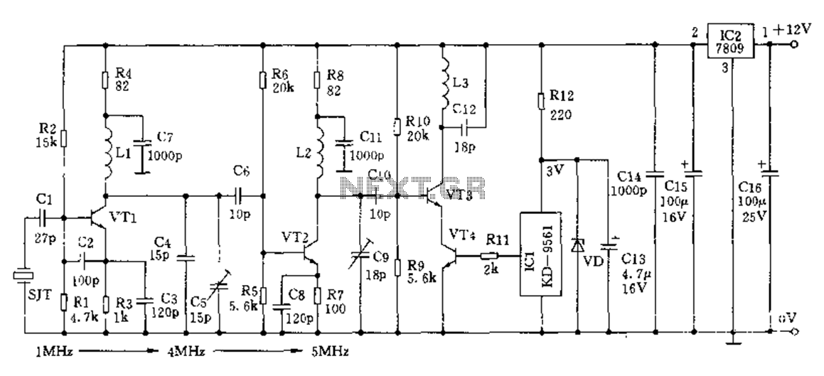
The crystal frequency stabilization of a frequency modulation circuit is illustrated below. The frequency modulation (FM) circuit utilizes crystal frequency stabilization to ensure precise frequency control and stability. This process involves the use of a quartz crystal oscillator, which...
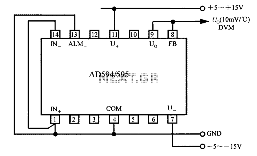
The AD594/595 can be configured to measure temperature in Celsius. In the circuit diagram, the IN+ and IN- terminals should be shorted to the COM terminal. The output voltage (Uo) has a temperature coefficient of 10 mV/°C, which can...
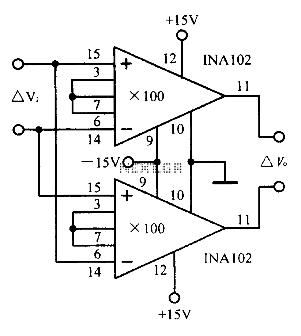
A differential input differential output amplifying circuit diagram. A differential input differential output (DIDO) amplifier is a type of operational amplifier configuration that is designed to amplify the difference between two input signals while rejecting any signals that are common...
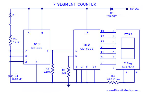
A simple seven-segment counter circuit with an LED display. This counter circuit diagram is designed using the IC CD 4033 as a counter, a 555 Timer IC, and a seven-segment LED display LT 543. The seven-segment counter circuit utilizes the...
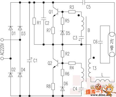
The saving lamp circuit features two main types: glass cover and exposed. The glass cover variants include three series: spherical, cylindrical, and processing types. The first two series consist of four variations: transparent, carved, engraved, and white. These lamps...
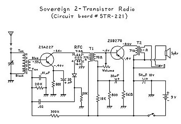
An analysis of certain radios reveals the impressive engineering by Japanese designers, particularly in creating a radio capable of driving a speaker with only two transistors. The first transistor (Q1) serves a dual function; it operates as an RF...