
Low-Cost Quad Op Amp Drives RF Modulator

The video circuit serves as an essential component in the processing of video signals, particularly in the context of broadcast standards such as NTSC and PAL. The audio-subcarrier notch filter is crucial for eliminating unwanted audio frequencies that may interfere with the video signal, thereby ensuring clarity and quality in transmission. The group-delay equalization is implemented to address the phase distortion that can occur due to the filtering process, allowing for a more accurate representation of the original signal.
The design incorporates multiple stages of all-pass filters, which are strategically configured to achieve the desired group-delay characteristics. The second-order stages provide a higher degree of control over the phase response, while the first-order stage offers additional fine-tuning capabilities. This multi-stage approach is vital for meeting the stringent requirements set forth by the ITU-470 standard, which governs the quality of broadcast video signals.
The adjustable output amplitude feature is particularly beneficial when interfacing with various RF video modulators, as it allows for flexibility in signal strength based on the specific application. The use of potentiometer R7 enables users to calibrate the output to match the input specifications of the modulator, ensuring optimal performance.
The notch filter's frequency response is determined by the values of the inductor L2 and capacitor C2, which set the center frequency of the notch. The depth and bandwidth of the notch are influenced by resistors R4, R5, and R6, allowing for customization based on the specific requirements of the application. The ability to achieve a notch depth greater than -16 dB indicates the effectiveness of the filter in suppressing unwanted frequencies.
Overall, this video circuit design exemplifies a sophisticated approach to video signal processing, ensuring compliance with industry standards while providing the necessary adjustments for varied operational scenarios.The video circuit illustrated in Figure 1 combines an audio-subcarrier notch filter and group-delay equalization as required by the ITU-470 standard. It also includes an amplitude-adjustment capability for driving an RF video modulator in NTSC applications.
(PAL operation requires a minor adjustment of the filter and all-pass values. ) For best per formance, the input should be driven from a low-impedance source, such as an op amp or active filter. Two second-order all-pass stages (U1a, R1, C1, L1 and U1c, R13, C3, L3) and a first-order all-pass stage (U1d, C4, R14) form a fifth-order group-delay equalizer that compensates for group delay introduced by the notch filter (U1b, R6, C2, L2).
Potentiometer R7 adjusts the output amplitude as required by the modulator in use. The notch frequency is set by L2 and C2, and the notch depth and bandwidth are set by R4, R5, and R6. Typical notch depth is greater than 16 dB ( Fig. 2 ). Flatness above 2. 5 MHz is ±0. 5 dB. 🔗 External reference
Related Circuits
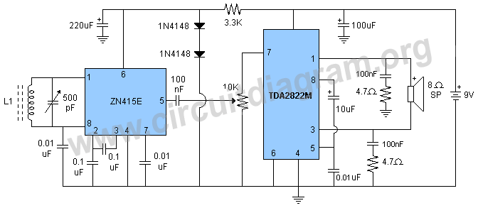
The RF detector circuit, RF amplifier circuit, and automatic gain control circuit (AGC) are integrated within the IC, allowing for the straightforward construction of a high-quality and sensitive AM receiver using this IC. The ZN415E IC is an advanced...
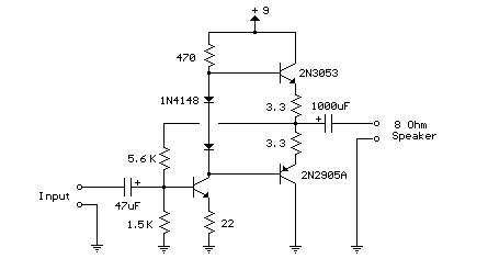
This weblog focuses on electronic circuit schematics, PCB design, DIY kits, and electronic project diagrams. The following describes a small audio amplifier, similar to those found in medium-sized transistor radios. The input stage is biased to ensure equal power...
Greetings to everyone. I am new to this forum, although I have previously used it to create a DIY projector. My knowledge of electronics is limited, and I am currently reading books to improve my understanding. The creation of a...
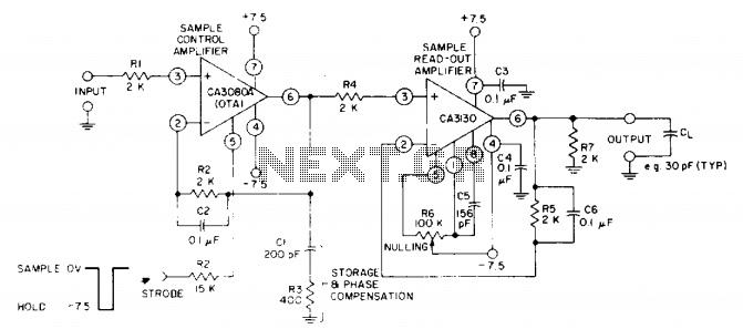
The circuit utilizes a CA3130 BiMOS operational amplifier as the sample-readout amplifier for the storage capacitor C1, while a CA3080A serves as the sample-control amplifier. Applications in linear systems that temporarily store analog data encompass digital voltmeter (DVM) systems,...
Here I propose a project of an AB class power amplifier, at its simplest, assembled with common components (not very expensive), based on traditional diagrams: a symmetrical differential input stage, a cascode stage driver, and a MOSFET output stage....
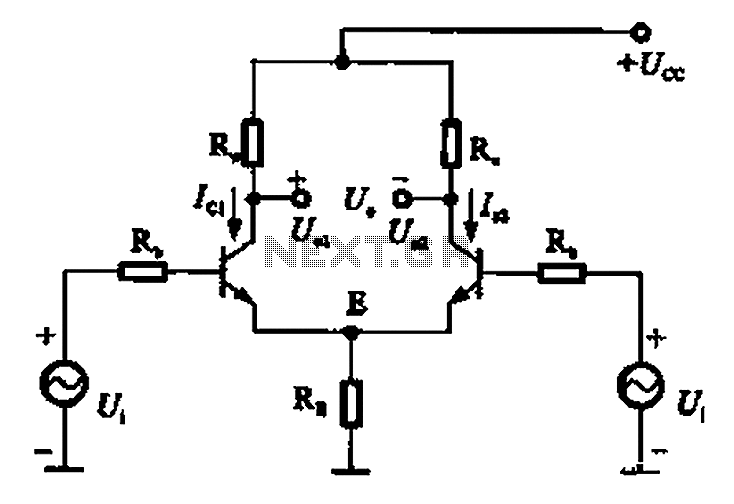
The common mode signal of an emitter-coupled differential amplifier circuit assumes that two equal small increases of the same polarity signal, referred to as the common mode signal, occur simultaneously. This results in an increase in the potential at...