
low power tia tunes gain 24 ghz

The transimpedance amplifier (TIA) is designed to convert input current signals into output voltage signals, making it particularly useful in applications such as photodetection and optical communication systems. The architecture incorporates a current-reuse stage, which enhances efficiency by allowing the same current to be used in multiple stages of amplification. This approach not only conserves power but also improves the overall gain performance of the amplifier.
The cascaded differential stage further contributes to the amplifier's performance by providing high linearity and better noise performance. This stage is crucial in maintaining signal integrity, especially in high-frequency applications such as 2.4 GHz, where signal degradation can occur due to various factors like thermal noise and flicker noise.
The continuous gain tuning range of 15 dB allows for flexibility in adjusting the amplifier's performance according to the specific requirements of the application. By fine-tuning the gain, the amplifier can accommodate different input signal levels while maintaining optimal noise performance.
The low noise figure of 1.061 dB is particularly noteworthy, as it indicates the amplifier's ability to minimize the addition of noise to the signal during amplification. This characteristic is essential in sensitive applications where signal fidelity is paramount.
Overall, this transimpedance amplifier design is well-suited for high-frequency applications, providing a combination of efficient power usage, adjustable gain, and low noise performance, which are critical for effective signal processing in modern electronic systems.This transimpedance amplifier employs a current-reuse stage and cascade differential stage to achieve a continuous gain tuning range of 15 dB and low noise figure of 1.061 dB at 2.4 GHz.. 🔗 External reference
Related Circuits

This circuit is designed for an LM1893 power line modem, which facilitates information transfer between remote locations using the power mains. The LM1893 serves as a power line interface for half-duplex (bi-directional) communication of serial bit streams employing various...
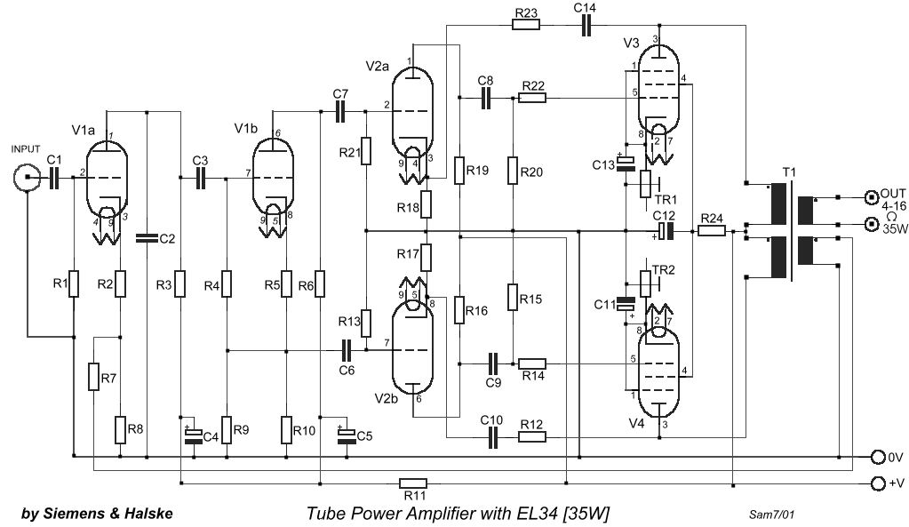
This is a classic design of a 35 W final amplifier utilizing two EL34 tubes in a push-pull configuration, developed by Siemens and Halske. The design dates back to March 24, 1953, and is identified by the code SV410/1....
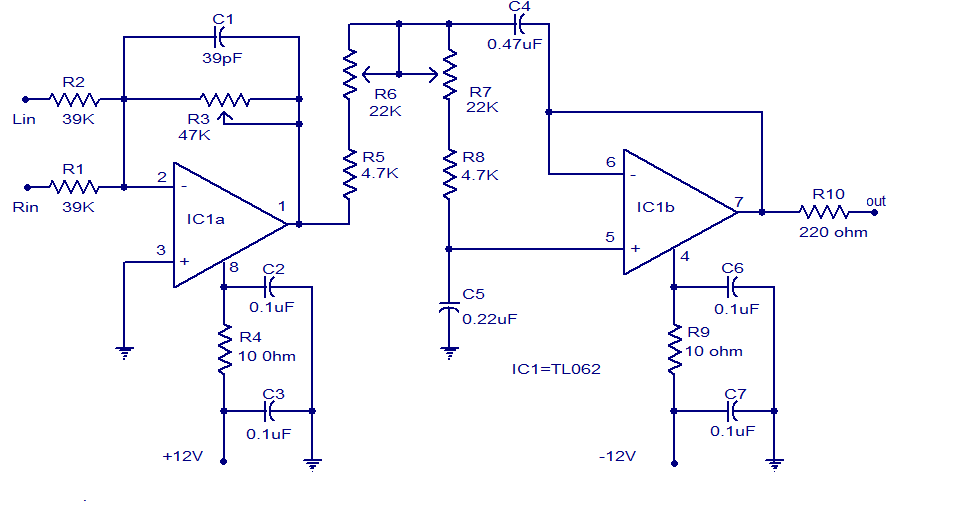
Many low-pass filter circuits for subwoofers are available, and this is another example. The circuit presented here utilizes the TL062 operational amplifier from STMicroelectronics. The TL062 is a dual high-input impedance JFET op-amp known for its low power consumption...
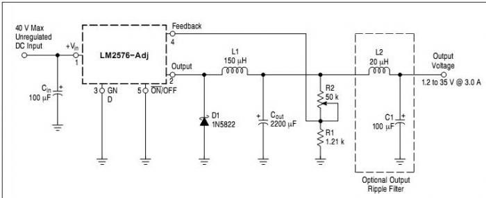
A simple lab power supply electronic project can be designed using this circuit diagram, which is based on the LM2576 monolithic integrated regulator that provides all the active functions for a step-down (buck) switching regulator. As seen in the...
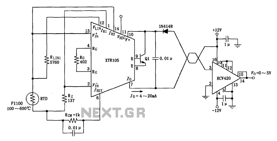
The circuit utilizes a Pt100 type resistance temperature detector (RTD). It operates within a temperature range of 100 to 600 °C, where the XTR105 outputs a current of 4 to 20 mA, and the RCV420 provides an output voltage...
One of the main features of the regulated power supply circuit being presented is that though fixed-voltage regulator LM7805 is used in the circuit, its output voltage is variable. This is achieved by connecting a potentiometer between common terminal...