
741 Timer
R3 and C can be selected with any values. Time delays ranging from fractions of a second to several hours can be achieved through careful selection. The time delay, which is independent of the supply voltage, is given by the formula T = R3 * C seconds, where C is in farads.
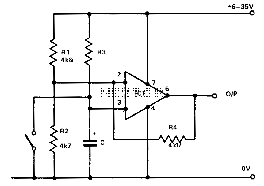
The circuit utilizes operational amplifiers (op-amps) configured in a comparator arrangement. Resistors R1 and R2 form a voltage divider that sets a reference voltage at the inverting input (pin 2) of the op-amp, typically at half of the supply voltage, allowing for effective comparison with the voltage at the non-inverting input (pin 3). The feedback resistor R4 is crucial for maintaining high input impedance, which is essential for accurate voltage detection and minimal loading on the input signal.
The capacitor C, in conjunction with resistor R3, creates a timing circuit that determines the delay before the output changes state. The charging of C through R3 follows an exponential curve, and the time constant (τ = R3 * C) dictates how quickly the capacitor charges to a level that exceeds the reference voltage set by R1 and R2.
This design allows for versatile applications in timing and control systems, where precise delays are necessary. By selecting different values for R3 and C, the circuit can be tailored to meet specific timing requirements. Additionally, the option to reverse polarity by swapping R3 and C adds flexibility to the design, allowing it to be adapted for various operational scenarios.
Overall, this configuration is a robust solution for applications requiring voltage comparison and timing functionality, suitable for use in various electronic systems, including timers, pulse generators, and other control circuits.Rl and R2 hold the inverting input at half supply voltage. R4 applies feedback to increase the input impedance at pin 3. Pin 3, the nonin-verting input, is connected to the junction of R3 and C. After the switch is opened, C charges via R3. When the capacitor has charged sufficiently for the potential at pin 3 to exceed that at pin 2 the output abruptly changes from 0 V to positive line potential. If reverse polarity operation is required, simply transpose R3 and C R3 and C can be any values. Time delays from a fraction of a second to several hours can be obtained by judicious selection. The time delay—independent of supply voltage —is 0CR seconds where C is in farads. 🔗 External reference
Related Circuits
The typical BPM range for music is between 40 and 240 BPM, corresponding to periods of 1500 ms and 200 ms, respectively. A BPM of 120 equates to a period of 500 ms. The circuit requires a resistor R4...
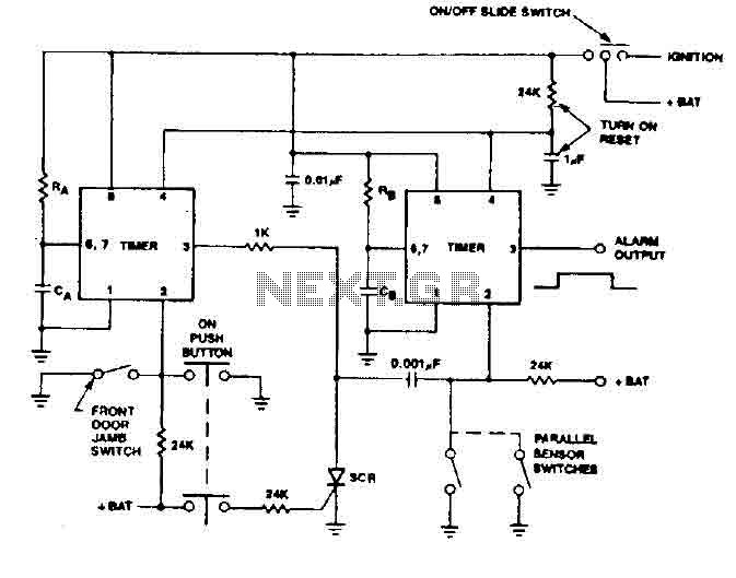
The 555 timer generates a reliable delay, enabling the driver to deactivate the alarm and eliminating the need for an external control switch that could be compromised. Additionally, the RCS prevents the activation of timer B unless it is...
In counter mode, it provides 1 Hz resolution up to 100 MHz. In timer mode, the maximum resolution is 0.0000001 Hz up to 1 Hz. The resolution decreases by one digit for each additional decade. Multiple frequency updates per...

28 LED Clock Timer Circuit. This is a programmable clock timer circuit that uses individual LEDs to indicate hours and minutes. Twelve LEDs can be arranged in a circle to represent the 12 hours of a clock face, along with...
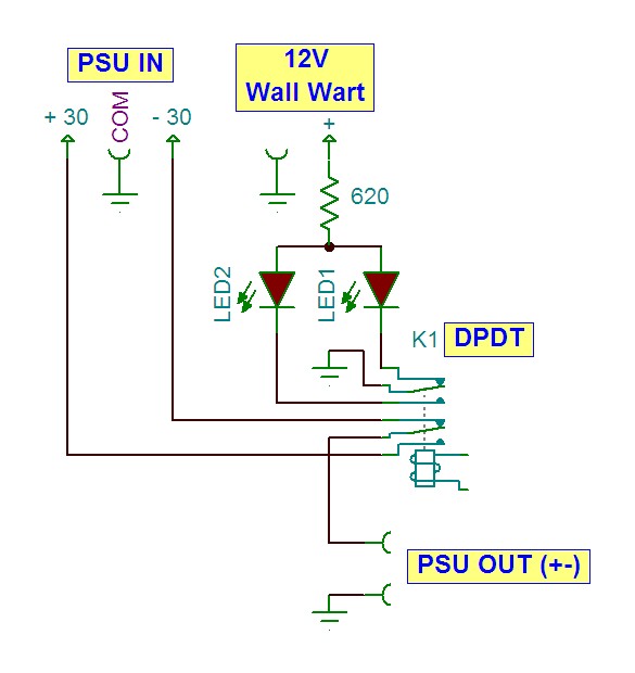
Thank you for the clarification. Since a dual (+-) supply is available, a single-pole double-throw (SPDT) relay will be sufficient. Is there a preference for a solid-state relay? A dual power supply configuration, typically indicated as +V and -V, allows...
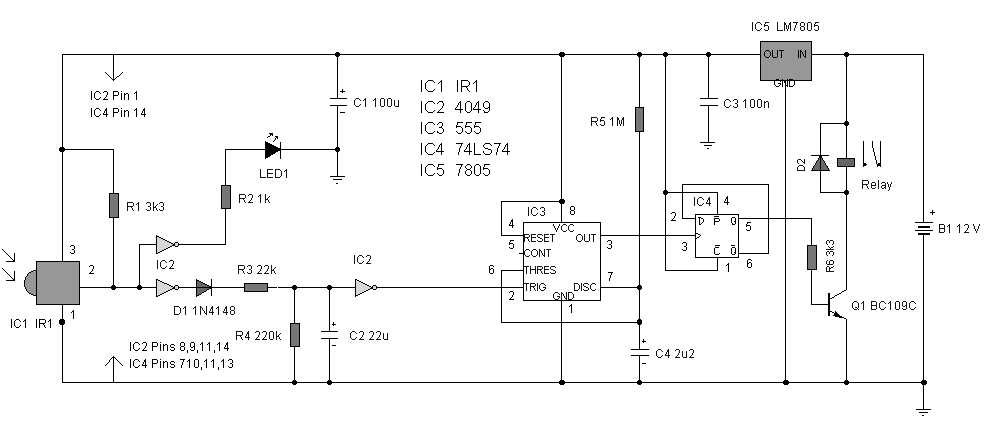
The circuit is designed to create a universal infrared switch with a single channel and ON/OFF functionality, operating in the frequency range of 36 kHz to 38 kHz, suitable for remote control applications. Infrared is a segment of the...