
Motor vehicle steering flasher 12

The motor vehicle steering flasher circuit serves as a critical component in automotive signaling systems, enabling drivers to communicate their intent to turn or change lanes effectively. The circuit operates by utilizing a simple oscillator configuration that alternates the current through the turn signal lamps, creating a flashing effect that is easily recognizable to other road users.
The resistors R1-R3 are integral in setting the timing characteristics of the oscillator circuit. The values of these resistors can be adjusted to modify the flash rate of the turn signals, allowing for customization based on vehicle requirements or regulatory standards. The choice of 1/4W carbon film or metal film resistors ensures reliability and stability in performance.
Capacitor C plays a vital role in the timing and stability of the oscillation. The use of a 25V electrolytic capacitor is appropriate for this application, providing sufficient voltage rating to handle the circuit's operational demands while maintaining compact size and efficiency.
The diode VD, specifically the 1N5402, is selected for its robustness and ability to handle higher current loads, ensuring that the circuit remains protected from voltage spikes and reverse polarity conditions. This diode is crucial for rectifying the current and allowing for proper operation of the transistors.
Transistors V1 and V2 are pivotal in controlling the oscillation and signal output. The selection of a silicon NPN transistor (3DGl2 or S8050) for V1 provides reliable switching capabilities, while the germanium PNP transistor (3AD30) for V2 allows for effective modulation of the current flow to the turn signal lamps. The combination of these transistors forms a complementary configuration that enhances the efficiency of the circuit.
Overall, the motor vehicle steering flasher circuit exemplifies a straightforward yet effective design that leverages basic electronic components to achieve reliable vehicle signaling. Proper selection and arrangement of the components ensure that the circuit functions correctly, providing essential safety features for automotive applications.The motor vehicle steering flasher described in the example uses high-power transistors as electronic switches, the circuit is simple, easy to make. The working principle The motor vehicle steering flasher is composed of the flash circuit resistors R1-R3.
Capacitor C, diode VD, transistors V1, V2, it is shown in Figure 7-21. S is the vehicle turn signal switch; HLl and HL2 are the left turn signal and right turn signal respectively. Before turning signal switch S (in the center), the oscillator circuit composed of vl, v2, and external RC components does not work. Placing S in the L or R position, the oscillation circuit works, V2 makes intermittent conduction with a certain frequency, Ll or HL2 is flashing.
Component selection RI-R3 selects 1/4W carbon film resistor or metal film resistors. C uses 25V electrolytic capacitors. VD uses lN5402 silicon rectifier diode. VI selects 3DGl2 or S8050 silicon NPN transistor; V2 uses 3AD30 germanium PNP transistors. 🔗 External reference
Related Circuits
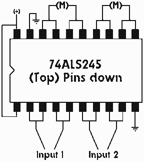
A motor driver is required in pretty much all walkers including all of my CW series walkers. You need to use it any time you need to supply more current to the motors because the circuit can't supply enough....
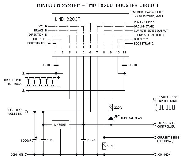
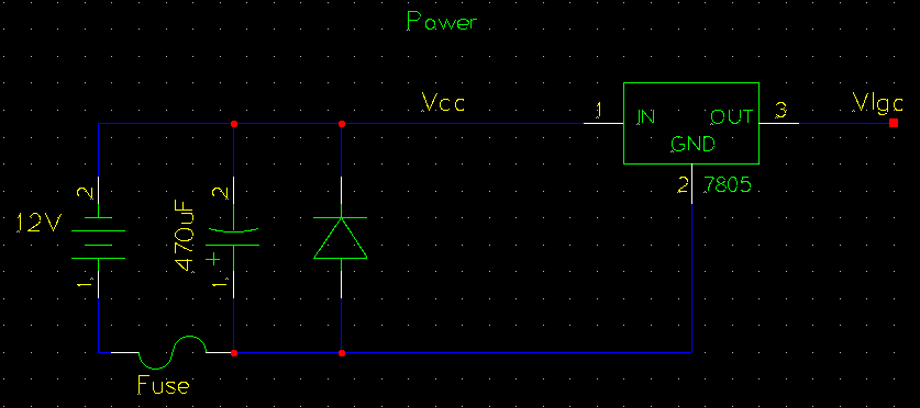
These circuits could be used as the basis for Model Railroad DCC Boosters or PWM motor controllers. The first schematic is for a basic 3 Amp - DCC Booster using the LMD 18200 CMOS, H-Bridge. Included in the design...
The circuit operates by using a clock signal to drive four D-flip-flops in the control section, which store the on/off state of each current direction for the two stepper motor coils. The flip-flops create a finite state machine (FSM)...
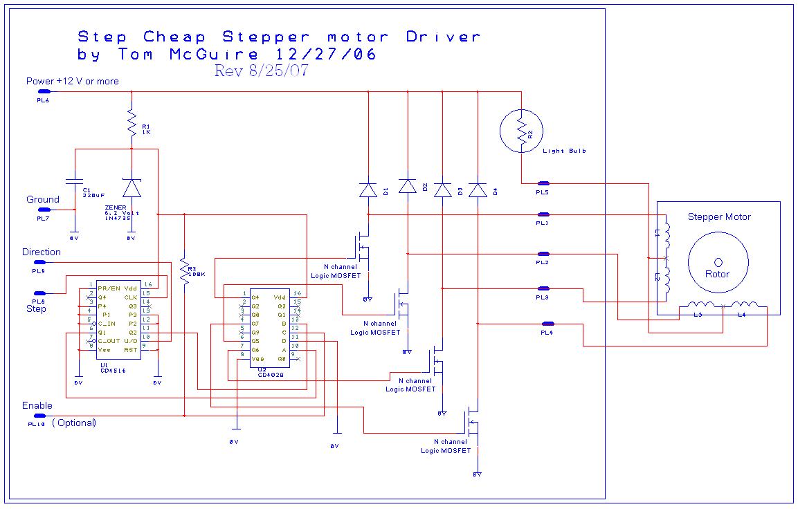
This circuit is designed to work with a variety of stepper motors, specifically 5 or 6 wire unipolar types. It operates within a voltage range of approximately 9 volts to 24 volts. A breadboard layout of the circuit is...
The circuit diagram is designed for precise control of DC motors. It converts DC voltage into a series of pulses, where the duration of each pulse... The circuit utilizes a pulse-width modulation (PWM) technique to regulate the speed and torque...

The circuit illustrated in Figure 3-85 features both manual and automatic control through the transfer switch SA. After initiating the motor Mi, an automatic start sequence is achieved via the time relay KT. The circuit employs a transfer switch (SA)...