
Negative Charge Pump with Ring Oscillator

The square wave oscillator circuit can be effectively constructed using a 555 timer or a ring oscillator made from CMOS inverters, each offering unique advantages. The 555 timer configuration typically includes a resistor-capacitor (RC) network that determines the frequency of oscillation. In contrast, the ring oscillator relies on the propagation delay of the inverters to generate oscillations.
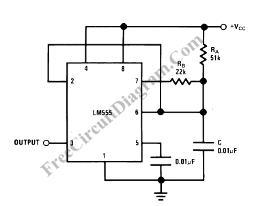
In the case of the charge pump circuit, the 555 timer's output at pin 3 alternates between high and low states, generating a square wave signal. This signal controls the charging and discharging of the 22µF capacitor, which is pivotal for the operation of the negative charge pump. During the high state, the capacitor charges through diode D1, storing energy. When the output transitions to low, the stored energy in the 22µF capacitor discharges through the 555 timer, effectively creating a path to ground. This discharge also influences the 100µF capacitor, which, due to the discharge path including diode D2, results in a negative voltage being established across it.
The use of CMOS technology in this application allows for low power consumption, but it is essential to consider the current limitations of the 4000 series logic family. If the application requires higher currents, alternative methods or components may be necessary. The overall design should ensure that the capacitors are rated appropriately for the voltage levels they will encounter, and the diodes must be selected to handle the reverse voltage and current requirements effectively. This configuration can be utilized in various applications, including signal generation, voltage inversion, and power supply circuits where a negative voltage is needed.In principle, the square wave oscillator doesn`t have to be a 555 timer, it could be a ring oscillator using inverters as you propose. In practice, using 4000 series CMOS logic for example, the negative output voltage produced would not be able to provide a great deal of current due to the current sourcing limitations of the IC.
If the amount of current required from the negative output created is small, maybe half a mA depending upon the supply voltage, I don`t see why using CMOS inverters for the oscillator wouldn`t work. Thanks a lot! I hope it`s not too much to ask, but could you explain the operation of the (negative charge pump part of the) circuit Cenoc May 5 `11 at 19:51 Pin 3 is the output of the 555, which will be a square wave between ground and the supply voltage.
When the output is high, the 22uF charges up through D1. When the 555 output goes low, the 22uF cap will discharge through the 555, through ground, the 100uF cap and D2, putting a negative voltage on the 100uF cap with respect to ground. Madmanguruman May 6 `11 at 2:20 🔗 External reference
Related Circuits
This circuit appears to be a Schmitt trigger oscillator. Based on the configuration of the resistors and capacitor, it is likely functioning as a sawtooth wave generator, with resistors R2 and R3 influencing the slope of the rising and...
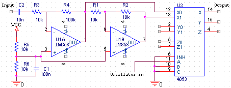
The multiplication operation required to generate a signal with a frequency equal to the difference of the input frequencies can be implemented in various ways. A multiplied signal typically appears when two signals are added and subsequently processed through...
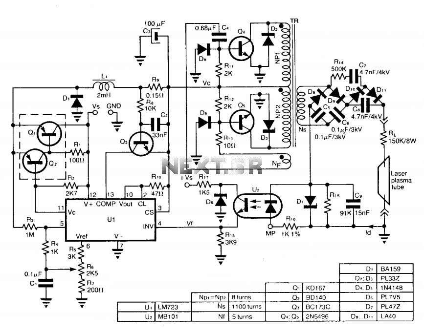
The circuit employs a free-running push-pull DC to DC high voltage converter to generate the required voltage for the laser plasma tube supply. The supply voltage (Vc) of this converter is regulated by a switch-mode power supply to maintain...

The following circuit illustrates the NE555 Timer used in an electronic scoring game circuit diagram. Features: The circuit consists of a timer integrated circuit (IC), along with various additional components. The NE555 timer is a versatile and widely used integrated...
A square wave oscillator utilizing the 555 integrated circuit (IC) can be configured to produce symmetric oscillation with a 50% duty cycle. Additional circuit configurations employ diodes to separate the charging and discharging paths. The 555 timer IC is a...
The pickups are connected to individual volume controls that feature push/pull functionality for coil tapping. They are routed to a 5-way switch before reaching the output jack. Additionally, a switch is desired to control the bridge pickup's activation when...