
Nonlinear Oscillator

The experiment aims to investigate the dynamics of a nonlinear circuit that simulates a driven pendulum, emphasizing the study of chaotic behavior and period doubling. The circuit's design builds upon previous works, specifically enhancing the phase locked loop (PLL) configuration. The PLL is a critical component in this setup, as it allows for the synchronization of the output frequency with an input reference signal, demonstrating key principles of nonlinear dynamics.
To initiate the experiment, the TDS220 oscilloscope must be set up to visualize the circuit's behavior. Understanding how to manipulate the oscilloscope's trigger settings and scaling options is vital for capturing accurate waveforms. The HP 35660A Dynamic Signal Analyzer should also be utilized to analyze the frequency response of the circuit components, particularly the low pass filter and integrator modules. These measurements provide insights into the circuit's performance and its ability to maintain synchronization under various conditions.
The assembly of the PLL modules should adhere to the provided block diagram, ensuring that one input of the integrator remains unused for future signal connections. The Wavetek 171 signal generator is connected through a switch-controlled attenuator to the reference input of the mixer, allowing for precise control over the reference wave amplitude and frequency. Careful monitoring of the reference wave's amplitude, set to -1.3 dBVrms or 860 mVrms, is essential as it directly influences the PLL's locking behavior.
During the experiment, the frequency range over which the PLL locks should be determined by systematically adjusting the frequency of the reference generator while observing the clock output of the VCO on the oscilloscope. The feedback resistance of the integrator should be set to 7700 ohms, as this value has been found to yield reasonable locking conditions. Observations should be made regarding the hysteresis effects around the locking range, as these can significantly impact the stability of the PLL.
It is advisable to approach the edges of the locking range cautiously to avoid losing synchronization. The experiment encourages exploration and experimentation with different configurations and parameters, allowing for a deeper understanding of the nonlinear dynamics involved. Additionally, the use of an oscilloscope to visualize the phase space motion of the simulated pendulum can enhance comprehension of chaotic behavior within the system.
Overall, this experiment provides a comprehensive examination of a nonlinear circuit modeled after a driven pendulum, offering valuable insights into the principles of chaos and synchronization in dynamical systems.The purpose of this experiment is to discover the properties of a nonlinear circuit which closely approximates a driven pendulum. It`s a great introduction to nonlinear phenomena such as period doubling and chaos. "Chaotic States and Routes to Chaos in the Forced Pendulum, " by D. D`Humieres, M. R. Beasley, B. A. Huberman, and A. Libchaber, Phys. Re v. A 26 3483 (1982). Our circuit is an improvement on theirs and is described in the section "Analysis of the Phase Locked Loop Circuit". Excerpts from Order Within Chaos by P. Berge, Y. Pomeau, and C. Vidal (Hermann and Wiley, Paris, 1984). This reference includes an introduction to the modem physics of dynamical systems. The following is a recommended sequence of steps for a long laboratory. Do not feel restricted to the operating parameters quoted in these notes, or even the methodology. Their main purpose is to help you get your feet wet. There is an enormous amount of investigation that can be done in this experiment, so feel free to focus on the parts you find most interesting, and also try out new ideas as they occur to you.
Familiarize yourself with the TDS220 oscilloscope if you have not used one before. Learn how to view and scale traces, how to manipulate the trigger settings, and how to use the cursors. The scope also has useful functions under the "measure" menu. Look over the "Getting Started Guide" for the HP 35660A Dynamic Signal Analyzer. Look at the spectrum and the time series measurement for the signal source running as a sine wave, a periodic chirp, and a random noise source.
Measure the frequency response of the low pass filter and the integrator modules of the oscillator. The procedure is described in Chapter 8 of the analyzer guide. Measure f0( = ‰0 / 2 ), the VCO frequency when the input is 0V (or shorted), and k( = ’ d ‰out / dVin), by applying a DC voltage to the VCO input (labeled "cont") and viewing the "clock" output on the spectrum analyzer. These are important parameters for understanding the circuit. Assemble the modules of the phase locked loop (PLL) following the block diagram below. Leave one input of the integrator unused; the drive signal will go there later. (Note: opening and shorting some terminals on this circuit give equivalent results, such as the integrator and VCO inputs.
However, the mixer will behave strangely if the "sine" input is left open. ) Next, connect the Wavetek 171 through a switch-controlled attenuator to the reference sine wave input of the mixer. It is useful to connect the same signal to a digital AC voltmeter for monitoring during the experiment.
Set the reference wave to an amplitude of -1. 3 dBVrms (measured on the spectrum analyzer) or 860 mVrms (measured on the voltmeter) while the frequency, fs( = ‰s / 2 ) is near f0. Find the frequency over which the PLL locks as follows: Externally trigger the scope from the sync output of the reference wave generator.
Monitor the output of the PLL by looking at the clock output of the VCO on the scope. Set the feedback resistance control on the integrator (R) to 7700. Scan the frequency of the generator and note the range of locking. Scan the R control on the integrator, noting the range over which locking occurs. You should compare the locking range with that expected (see the "Equilibrium Phase and Conditions for Locking" subsection below). There is substantial hysteresis near the edges of the locking range. If the PLL becomes unlocked because you took too large a step in reference frequency you should return to the center of the locking range and approach the edges more cautiously.
Reasonable settings for most of the measurements are: R = 7700, reference wave amplitude = 860 mVrms, fs = fL. You might enjoy learning about PLLs and their applications in the excerpt from The Art of Electronics.
An oscilloscope can be connected so that you can watch the phase space motion of the pendulum being simulated. The integrato 🔗 External reference
Related Circuits
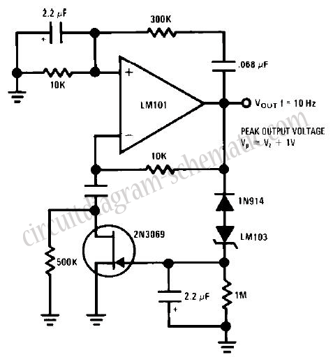
This circuit is a Wien Bridge Sine Wave Oscillator. The primary challenge in generating a low distortion, constant amplitude sine wave is to achieve the appropriate loop gain in the amplifier. By utilizing the 2N3069 JFET as a variable...
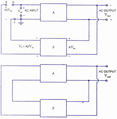
A feedback amplifier with a closed-loop gain, Af, greater than unity can be achieved through the use of positive feedback. This condition also fulfills the phase requirement, leading to the operation of an oscillator circuit. An oscillator circuit generates...
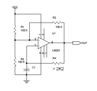
This circuit utilizes the Op-Amp LM301 to generate a simple square wave. The LM301 operates with a power supply range of 3 V to 36 V and can handle a maximum frequency of 325 kHz. The oscillation frequency is...
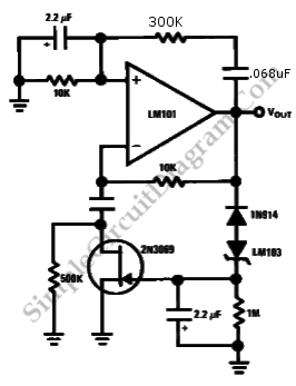
Achieving the appropriate amplifier loop gain is a significant challenge in generating a low distortion, constant amplitude sine wave. Nevertheless, this issue can be addressed with... Amplifier loop gain is a critical parameter in the design of audio and signal...

An op-amp based Colpitts oscillator in Multisim displays a "timestep too small" error when the run button is pressed. Despite extensive research and attempts to resolve the issue, the error persists. The design features a C-L-C pi circuit that...
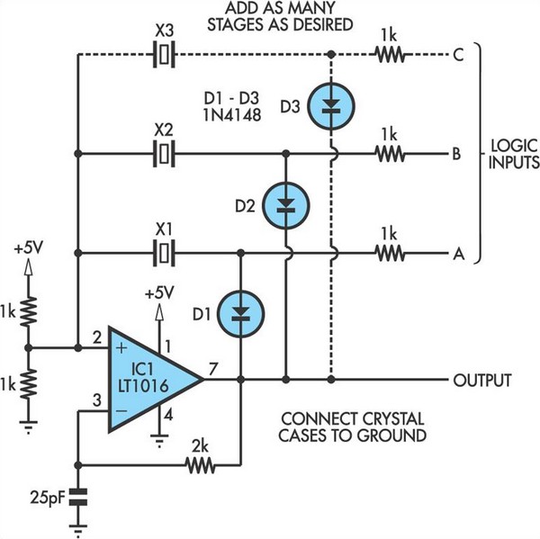
This oscillator circuit allows crystals to be electronically switched by logic commands. To understand the circuit, it is helpful to initially disregard all crystals and consider all diodes as shorts while their associated 1kΩ resistors are treated as open....